
Professional PCB manufacturing and assembly
Building 6, Zone 3, Yuekang Road,Bao'an District, Shenzhen, China
+86-13410863085Mon.-Sat.08:00-20:00

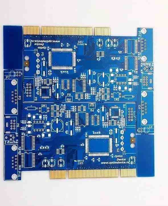
Verification of PCB design rules in shared development
I used to think that development is just a software development method with specific rules and processes. On the surface, the hardware design process seems to be rigid, but any design process aims to enable the team to adapt to changes throughout the product development cycle. In fact, the core idea of development can be applied to any business process facing change risk, including hardware design.
If properly implemented, the development workflow can help prevent unnecessary redesign and ensure that product functions are closely aligned with customer needs. In electronic and hardware design, the idea of the method depends on PCB design rule verification in the whole product development process. This helps the design team quickly validate design requirements and propose design changes during each sprint.
Rule driven workflow
Workflow is designed to be adaptive and adapt to changes throughout the design process. The documentation phase at the beginning of any development method provides an opportunity for designers to define important design rules and constraints before the design starts. You can code these rules into your design software at the beginning of the design phase. These design rules can follow the industry standards for specific applications, or exceed the standard rules to improve the performance and reliability of products.
The rules and constraints in the design tools help ensure that your schematic design and PCB layout meet your requirements when you build a circuit board. Some design software packages only allow you to check the design in batches according to rules and constraints, so most design processes need to check the design rules at specific points in the design process. As part of the workflow, it is best to review your design against rules and constraints as you work toward design milestones during each design sprint.
The best design tools will check your layout in real time according to the design rules, allowing you to identify errors when laying out the circuit board. Unified interactive and automatic interactive routing tools are perfect in this regard, because they check your routing choices in real time according to your design rules. You can immediately identify gap violations, length mismatch violations, and ensure that your routing maintains consistent geometry throughout the interconnect.
Imagine manually checking each of these traces according to your design rules
These same ideas apply to embedded systems; Before compiling the code and deploying it to the prototype, using the correct embedded software tools can help you quickly identify errors or problems in the code by comparing the code with important coding standards (such as MISRA and CERT C in TASKING). Explanation of PCB assembly and PCB processing manufacturers: share the verification of PCB design rules under development.
Overcoming the Limitation of PCB Design Rule Verification through Simulation
Although design rules are important to ensure that your design can be manufactured and meet important design criteria, they do not guarantee the electrical performance of your system. Just because your design conforms to basic industry standards and manufacturing guidelines does not mean it will provide the electrical performance you need. Here, performing simulations at various points during design can help you identify layout or component changes, thereby improving signal integrity in your design.
Before starting a new design, the simulation of important circuits is usually run in SPICE or other circuit simulators. This helps to validate design requirements and recommend changes before starting schematic design and layout. After verification, the linear design process usually requires simulation to be performed at a specific point (usually after the design is completed). This is partly because many simulators exist outside the design software itself, and it only takes too much time to call multiple simulators in the design phase.
With integrated design software, you can immediately run the simulation of schematic and PCB layout without exporting the design to an external program. This makes integrated software an ideal choice for design, because you don't have to wait until the layout is complete to run the simulation. When your simulation tools are integrated into your design software, you can quickly diagnose signal integrity problems during continuous design sprints as part of your workflow.
One of the many electrical simulations you can perform during the design process
Adapt to changes in PCB design
The simulation results inform two aspects of design modification: exchanging components and changing layout. Simulating your equipment at the schematic and component levels helps you determine whether the components you select can provide the electrical performance specified in the design requirements. You can then quickly replace components as needed, or you can modify your electronic schematics to resolve any signal integrity issues.
Even if the schematic diagram is corrected according to the simulation results, you cannot guarantee the performance if the PCB design rules are not verified for the layout. Simulations of layouts are also important because they can help you identify layout choices that cause crosstalk, EMI sensitivity, and other signal integrity issues. As part of the workflow, this enables you to identify specific changes required in the layout, enabling you to quickly resolve these changes during each design sprint. This is better than waiting for the design to be completely completed, which is usually done during the linear design process. In this case, any layout change may be large and time-consuming, and this should be avoided as far as possible.


Just upload Gerber files, BOM files and design files, and the KINGFORD team will provide a complete quotation within 24h.