
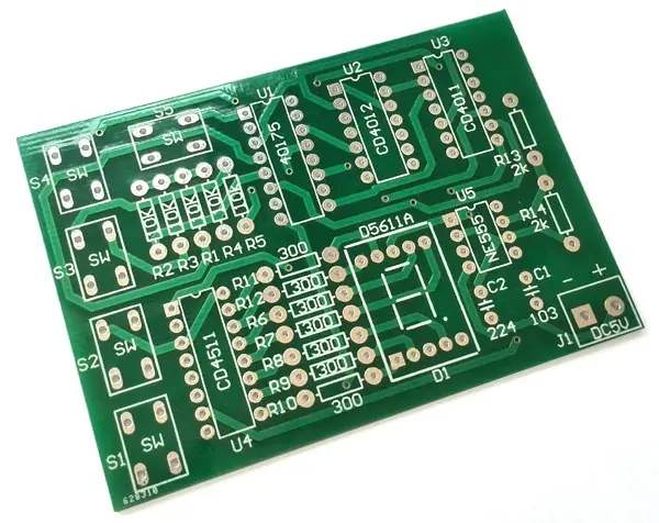
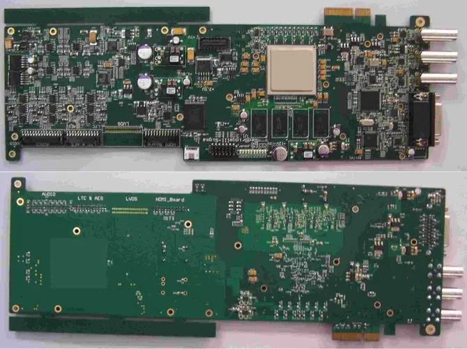
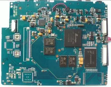
Professional PCB manufacturing and assembly
Building 6, Zone 3, Yuekang Road,Bao'an District, Shenzhen, China
+86-13410863085Mon.-Sat.08:00-20:00

Simulation "Softening" of New Challenges in High Speed and High Density PCB Design
PCB assembly and PCB processing manufacturers explain the new challenges faced by high-speed and high-density PCB design through simulation "soft" your design
Simulation is the test of virtual prototype that takes all aspects into account. As the design is becoming more and more complex, engineers cannot implement every scheme. At this time, they can only use advanced simulation instead of test to judge.
Today's system design, in addition to the challenges brought by high-speed and high-density circuit boards, the pressure of rapid product launch makes simulation an indispensable means of system design. The designer hopes to use advanced simulation tools to find out problems in the design phase, so as to complete the system design with high efficiency and quality.
In the traditional circuit board design, engineers rarely use the means of simulation. More often, we use the reference design and design guidance rules (i.e. white paper) provided by upstream chip manufacturers, combine the actual experience of engineers to design, and then repeatedly test the prototype designed and produced, find out problems, and modify the design. This cycle will continue until the problems are basically solved. Even if simulation tools are occasionally used for design, they are only limited to local circuits. Modifying the circuit means a delay in time, which is unacceptable under the pressure of the rapid introduction of products. Especially for large systems, a small modification may need to overturn the entire design. As the saying goes, "one change affects the whole body", the loss to circuit board manufacturers is incalculable.
It is difficult to guarantee product quality, uncontrollable development cycle, and excessive dependence on engineers' experience... These factors make it difficult for the above design methods to meet the challenges brought by increasingly complex high-speed and high-density PCB design, so they must be solved with advanced simulation tools. "The design scheme given by the upstream chip manufacturers is based on their own templates, while the products of the system manufacturers cannot be exactly the same as those of the upstream manufacturers; at the same time, the design requirements of one chip may contradict those of another, so the design scheme must be determined through simulation." Chen Lanbing said.
In a sense, simulation is to enable software to complete functional evaluation on virtual prototypes that can only be completed by testing physical prototypes. It is a more "soft" and more economical solution.
However, the simulation of high-speed and high-density circuit boards is different from the traditional simulation. "Traditional simulation is done for schematic diagrams. It just adds excitation and looks at the output to judge whether the function is correct. High speed simulation is to look at the performance of the design on the premise of correct functions. It aims at both schematic diagrams and PCB design." The simulation tool can be used to judge which scheme is closer to the actual demand. On the basis of meeting the performance requirements, it can judge which scheme has lower cost, and find a balance between the performance design and the system cost. Yulif said: "Using simulation tools, we can judge whether the direction of system improvement is correct, point out the direction for design, improve the success rate of the first board, and make the product go to the market faster. However, no matter how close the simulation results are to the test results, it can not replace the actual test system."
Testing is a true judgment of system performance including all real environment factors. However, simulation is a "test" of virtual prototype, which is aimed at certain specific conditions. No tool can take all real conditions into account and simulate at the same time. However, with the development of technology and the continuous improvement of tools, the approximation of simulation results and actual test results is getting higher and higher, which is more and more significant for the design. At the same time, it also puts forward higher requirements for engineers. Although the tools are more and more easy to use, the judgment and improvement methods of simulation results depend on the technical level and theoretical basis of engineers.
At present, in high-speed PCB simulation, the effect of EMC/EMI is the least ideal. This is because for high-speed systems, due to the influence of via effect, three-dimensional modeling of the system is required to effectively simulate the real environment. However, for such a huge and complex system as PCB, it is very difficult to model it in 3D. At present, the method of expert inspection is mainly adopted, which is to transform the EMC/EMI problem into PCB layout and routing rules according to the international general standards.


Just upload Gerber files, BOM files and design files, and the KINGFORD team will provide a complete quotation within 24h.