
Professional PCB manufacturing and assembly
Building 6, Zone 3, Yuekang Road,Bao'an District, Shenzhen, China
+86-13410863085Mon.-Sat.08:00-20:00

Expert solutions to high-speed circuit board design methods Part II
10. Test point generation Can test points automatically generated by software on high-density printed boards meet the test requirements of mass production in general? Will adding test points affect the quality of high-speed signals?
Expert answer:
In general, whether the software automatically generates test points to meet the test requirements must depend on whether the specification of additional test points meets the requirements of the test equipment. In addition, if the routing is too dense and the specification for adding test points is strict, it may not be possible to automatically add test points to each segment of the line. Of course, you need to manually complete the place to be tested.
Whether it will affect the signal quality depends on the way of adding test points and how fast the signal is. Basically, the additional test points (not using the existing via or DIP pin as the test point) may be added to the line or pulled out of a small section of line. The former is equivalent to adding a very small capacitor on the line, while the latter has an extra branch. Both of these two conditions will affect the high-speed signal more or less. The degree of influence is related to the frequency speed of the signal and the edge rate of the signal. The magnitude of the impact can be known through simulation. In principle, the smaller the test point, the better (and of course, meet the requirements of the test machine). The shorter the branch, the better.
11. How to select PCB board? How to select PCB board? How to avoid high frequency interference of high-speed data transmission to surrounding analog small signals? Are there any basic design ideas?
Expert answer:
The selection of PCB board must achieve a balance between meeting the design requirements and mass production and cost. The design requirements include electrical and mechanical parts. This material problem is usually important when designing very high-speed PCB boards (frequencies greater than GHz). For example, the commonly used FR-4 material, dielectric loss at several GHz frequencies, may have a great impact on signal attenuation, and may not be suitable. As far as electricity is concerned, pay attention to whether the dielectric constant and the dielectric loss are applicable at the designed frequency.
The basic idea to avoid high-frequency interference is to minimize the interference of high-frequency signal electromagnetic field, which is called crosstalk. You can increase the distance between high-speed signal and analog signal, or add ground guard/hunt traces beside analog signal. Attention shall also be paid to the noise interference of digital ground to analog ground.
12. What does each layer of a PCB mean? As we all know, a PCB includes many layers, but I still don't know the meaning of some layers.
Mechanical, keepoutlayer, topoverlay, bottomoverlay, toppaste, bottompaste, topsolder, bottomsolver, drillguide, drilldrawing, and multilayer do not know their exact meanings. I hope you can give me some advice.
Expert answer:
In terms of EDA software, there are many terms that do not have the same definition. The following is a literal explanation of the possible meaning.
Mechnical: general multi finger plate type machining dimension marking layer
Keepoutlayer: defines the area that cannot be used for routing, punching (via) or swinging parts. These restrictions can be defined separately.
Topoverlay: I can't tell its meaning literally. Provide more information for further discussion.
Bottom overlay: I can't tell its meaning literally. More information can be provided for further discussion.
Toppaste: The top layer needs to expose the solder paste on the copper skin.
Bottompaste: The bottom layer needs to expose the solder paste on the copper skin.
Topholder: It refers to the top layer of solder mask to avoid possible accidental short circuit during manufacturing or future maintenance
Bottomsolder: refers to the bottom layer of solder mask.
Drillguide: It may be a table of symbols and numbers of different aperture sizes.
Drilldrawing: refers to the hole bitmap. Each different hole diameter will have a corresponding symbol.
Multilayer: There should be no separate layer, which refers to multilayer boards, for single panel and double-sided boards.
13. Grounding connection problem A system is often divided into several PCBs, including power supply, interface, motherboard, etc. The ground wires between the boards are often interconnected, resulting in the formation of many loops, such as low-frequency loop noise. How can I solve this problem?
Expert answer:
When the signal or power supply between the interconnects of PCB boards acts, for example, if board A has power or the signal is sent to board B, there must be an equal amount of current flowing back from the stratum to board A (this is Kirchoff current law). The current in this stratum will flow back to the place with the lowest impedance. Therefore, the number of pins allocated to the formation at each interface, whether the power supply or signal is connected, cannot be too small to reduce impedance, which can reduce the noise on the formation. In addition, it is also possible to analyze the entire current loop, especially the part with large current, and adjust the grounding method of the stratum or ground wire to control the current path (for example, make a low impedance at a certain place to let most of the current flow from this place), so as to reduce the impact on other sensitive signals.
14. How to estimate the characteristic impedance. (1) Can you provide some empirical data, formulas and methods to estimate the impedance of the wiring. (2) When impedance matching requirements cannot be met, it is better to add a matching resistor in parallel at the end of the signal line or in series on the signal line. (3) Can a ground wire be added in the middle of the differential signal line.
Expert answer:
1. Two frequently referenced characteristic impedance formulas are provided as follows:
a. Microstrip
Z={87/[sqrt (Er+1.41)]} ln [5.98H/(0.8W+T)] where W is the line width and T is the copper sheet for wiring
Thickness, H is the distance from the wiring to the reference plane, Er is the dielectric constant of the PCB material. This formula can only be applied when 0.1<(W/H)<2.0 and 1<(Er)<15.
b. Stripline
Z=[60/sqrt (Er)] ln {4H/[0.67p (T+0.8W)]} where H is the distance between two reference planes, and
The routing is located in the middle of the two reference planes. This formula can only be applied when W/H<0.35 and T/H<0.25. It is better to use simulation software to calculate accurately.
2. There are several factors to consider when selecting the termination method:
a. The architecture and strength of the source driver.
b. The power consumption.
c. This is the most important consideration for the impact of time delay.
Therefore, it is hard to say which termination method is better.
3. Generally, the differential signal cannot be connected with a ground wire. Because the most important point of differential signal application principle is to use the benefits of coupling between differential signals, such as flux cancellation, noise immunity, etc. If a ground wire is added in the middle, the coupling effect will be destroyed.
15. Calculation of characteristic impedance I think that the microstrip line and stripline model of the characteristic impedance of the signal line should refer to the ground plane. Now I want to ask how to calculate the characteristic impedance of the signal line on the top floor if the copper sheet below the signal line is hollowed out and there is no reference ground plane? In addition, I see some data that the power plane can also play the same role as the ground plane in eliminating the noise on the signal line, right?
Expert answer:
The interaction between electric field and magnetic field without reference plane is different from that with reference plane, and this interaction will affect the value of characteristic impedance. At present, most of the formulas for calculating the characteristic impedance assume that there is a reference plane. I haven't seen such formulas without a reference plane. However, TDR (Time Domain Reflectometer) can be used to measure the actual board to obtain the characteristic impedance without reference plane.
The reason for the noise on the signal line is that the energy of electric field and magnetic field generated by signals on other lines is transmitted to the infected signal line through the mutual induction and mutual capacity. The power plane and ground plane are basically metal planes, so they have shielding effects on electric and magnetic fields.
16. Technical books and materials on high-speed PCB design Can you introduce some foreign current technical books and materials about high-speed PCB design level, processing ability, processing level, processing materials and related technologies?
Expert answer:
Nowadays, high-speed digital circuits are used in communication networks, computers and other related fields. In terms of communication network, the working frequency of PCB board has reached GHz, and the number of layers is up to 40 as far as I know. Computer related applications are also due to the progress of chips. The maximum operating frequency on the board has reached more than 400MHz (such as Rambus), no matter for ordinary PCs or servers. In response to the demand for high-speed and high-density routing, the demand for blind/buried vias, mirrovias and build up processes is also increasing. These design requirements can be mass produced by manufacturers.
Here are some good technical books:
1.Howard W. Johnson,“High-Speed Digital Design - A Handbook of Black Magic”;
2.Stephen H. Hall,“High-Speed Digital System Design”;
3.Brian Yang,“Digital Signal Integrity”;
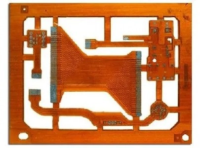
17. Design and processing of flexible circuit board Our company plans to use flexible circuit board design to solve the problem of signal transmission and circuit board interconnection in small imaging systems. Does the rigid flexible panel design require special design software and specifications? In addition, where can we undertake such PCB processing in China? thank you.
Expert answer:
Flexible Printed Circuit can be designed with general PCB design software. It is also produced by FPC manufacturers in Gerber format. Since the manufacturing process is different from that of general PCBs, each manufacturer will limit the minimum line width, minimum line spacing and minimum aperture (via) according to their manufacturing capacity. In addition, copper sheet can be laid at the turning point of the flexible circuit board for reinforcement. As for the manufacturer, you can search for "FPC" as a keyword on the Internet.
18. PCB wiring adjustment I would like to ask a question: because the machine cloth is not satisfactory, it takes time to adjust it. I usually use manual wiring. Most PCB boards now use chips with high pin density to package chips, and for those with buses (ABUS, DBUS, CBUS, etc.), the leads should be as short as possible because of the high operating frequency Naturally, very dense signal lines are evenly distributed on boards with small area. I now feel that it takes more time to adjust these dense signal lines. First, adjust the distance between lines to make them as uniform as possible. Because in the process of wiring, it is generally necessary to change lines from time to time. The spacing of each laid line shall be re uniform after each change. The more we get to the end, the more this happens. The second is to adjust the width of the line to accommodate new lines as much as possible in a certain width. Generally, there are many bends on a line, and each bend is a segment. Manual adjustment can only be performed segment by segment, which also takes time. I think if I can pull the wire manually according to my idea in the wiring process, the software can help me automatically adjust from these two aspects after that. Or even if the cloth is finished, if you want to change the thread, you should also change it roughly, and then let the software adjust it. Even, in the end, I think it is necessary to adjust the packaging of components, that is, the whole piece of wiring needs to be adjusted, and let the software do it. That would be much faster I use Protel98. I know that this software can automatically and evenly adjust the distance of component packaging, but can not automatically adjust the line spacing and line width. Maybe I don't know how to use some of these functions, or there are other ways. Please consult me here.
Expert answer:
Line width and line spacing are two important factors affecting the routing density. In general, when designing boards with high operating frequency, the characteristic impedance of the wiring needs to be determined before wiring. The characteristic impedance will determine the line width when the PCB stack is fixed. The line spacing is absolutely related to the crosstalk. The minimum acceptable line spacing depends on whether the crosstalk can affect the signal time delay and signal integrity. The minimum line spacing can be obtained by pre simulation of simulation software. That is to say, before wiring, the required line width and minimum line spacing should have been determined, and should not be changed at will, because it will affect the characteristic impedance and crosstalk. This is why most EDA routing software will not change the line width and minimum line spacing when making automatic routing or adjustment.


Just upload Gerber files, BOM files and design files, and the KINGFORD team will provide a complete quotation within 24h.