
Professional PCB manufacturing and assembly
Building 6, Zone 3, Yuekang Road,Bao'an District, Shenzhen, China
+86-13410863085Mon.-Sat.08:00-20:00

PCB Layout and Serpentine Processing for Beginners
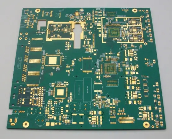
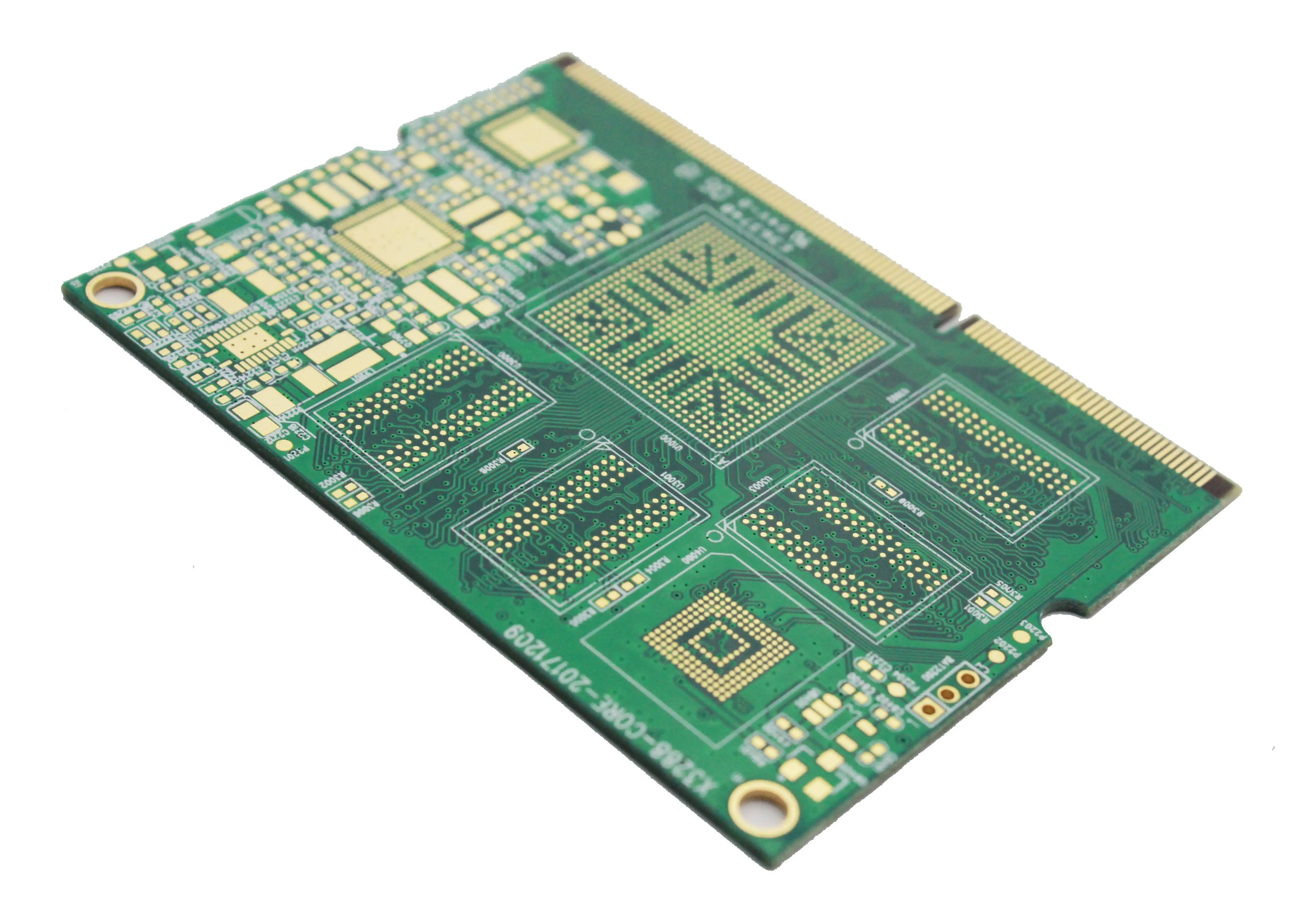
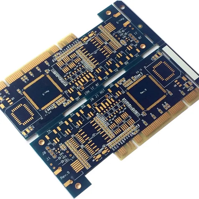
PCB device layout is a very skillful thing, but if you master its principles, everything will become very simple. The following are some PCB device layout principles summarized in daily life.
1. The I/O driver shall be close to the edge of the printed board and the outlet connector as far as possible;
2. According to the reasonable division of electrical performance, it is generally divided into: digital circuit area (that is, to avoid interference and generate interference) and analog circuit area
(Fear of interference), power drive area (interference source);
3. For components with high quality, the installation position and strength shall be considered; The heating element shall be placed separately from the temperature sensing element, and thermal convection measures shall be considered when necessary;
4. Circuits with the same function shall be placed as close as possible, and all components shall be adjusted to ensure the most concise connection; At the same time, adjust the relative position between the function blocks to make the connection between the function blocks the most concise;
5. The I/O driver shall be close to the edge of the printed board and the outlet connector as far as possible;
6. The clock generator (such as crystal oscillator or clock oscillator) shall be as close as possible to the device using the clock;
7. The relay coil shall be equipped with a discharge diode (1N4148 is enough);
8. The layout should be balanced, dense and orderly, not top heavy or heavy
9. A decoupling capacitor shall be added between the power input pin and the ground of each integrated circuit (generally, a monolithic capacitor with good high-frequency performance is used); When the circuit board space is dense, a tantalum capacitor can also be added around several integrated circuits.
Some Suggestions for PCB Factory in Designing and Handling Serpentine
1. Try to increase the distance (S) of parallel line segments, which shall be at least greater than 3H. H refers to the distance from the signal line to the reference plane. Generally speaking, it is to route around a big bend. As long as S is big enough, it can almost completely avoid mutual coupling effects.
2. Reduce the coupling length Lp. When the twice Lp delay is close to or exceeds the signal rise time, the crosstalk generated will reach saturation.
3. The signal transmission delay caused by serpentine line of strip line or embedded micro strip is less than that of micro strip. In theory, the stripline will not affect the transmission rate due to differential mode crosstalk.
4. For high-speed signal lines and signal lines with strict timing requirements, try not to take serpentine lines, especially in small areas.
5. Snakelike routing at any angle can be often used to effectively reduce mutual coupling. PCB assembly, PCB design, and PCB processing manufacturers explain the PCB device layout and serpentine processing that beginners must know.
6. In the design of high-speed PCB, the serpentine line has no so-called filtering or anti-interference ability, and it can only reduce the signal quality, so it is only used for timing matching and has no other purpose.
7. Sometimes spiral routing can be considered for winding, and simulation shows that its effect is better than that of normal serpentine routing.


Just upload Gerber files, BOM files and design files, and the KINGFORD team will provide a complete quotation within 24h.