
Professional PCB manufacturing and assembly
Building 6, Zone 3, Yuekang Road,Bao'an District, Shenzhen, China
+86-13410863085Mon.-Sat.08:00-20:00

Several problems that engineers should pay attention to when designing PCB
The circuit board assembly manufacturer explains several problems that engineers should pay attention to when designing PCB circuit boards
The schematic design before single panel proofing is a preliminary preparation. When drawing the schematic, pay attention to the connection of each file as a whole in the hierarchical design, which is also important for future work. Due to the difference of software, some software may appear to be connected but not actually connected (in terms of electrical performance). If you do not use the relevant detection tools to detect, in case of a problem, it will be late to find out when the board is ready. Therefore, we have repeatedly stressed the importance of doing things in order and hope to draw everyone's attention. The circuit board assembly manufacturer explains several problems that engineers should pay attention to when designing PCB circuit boards. The schematic diagram is based on the project designed by PCB. As long as the electrical connection is correct, there is nothing to say. Here I summarize some experience to share with you:
l. Make Physical Border
The closed physical frame is a basic platform for future pcb component layout and routing, and also a constraint for automatic layout. Otherwise, components coming from the schematic will be at a loss. But you must pay attention to the accuracy here, otherwise you will have a lot of trouble in the future. Also, it is better to use arc at the corner, which can avoid sharp corner scratching workers on the one hand and reduce the stress effect on the other. In the past, one of my products was always broken in the process of transportation by a few machines. It would be better to use circular arc instead.
2. Introduction of components and networks
It should be easy to draw components and networks into the drawn border, but problems often occur here. Be careful to solve the problems one by one according to the prompted errors, otherwise it will take more effort later. The problems here are generally as follows:
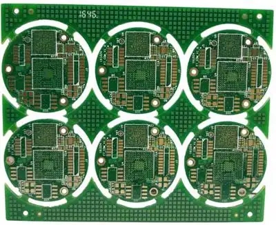
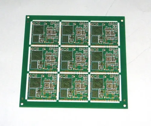
The package form of the component cannot be found, the component network has problems, and there are unused components or pins. It is suggested that these problems can be solved quickly. PCB PCB proofing
3. Layout of components
The layout and routing of components have a great impact on the life, stability and electromagnetic compatibility of products, which should be paid special attention to. Generally speaking, the following principles should be followed:
3. l Placing order
First place the components at fixed positions related to the structure, such as power sockets, indicator lights, switches, connectors, etc. After placing these components, use the LOCK function of the software to lock them, so that they will not be moved by mistake in the future. Then place special components and large components on the circuit, such as heating components, transformers, ICs, etc. Finally, place the small device.
3.2 Pay attention to heat dissipation
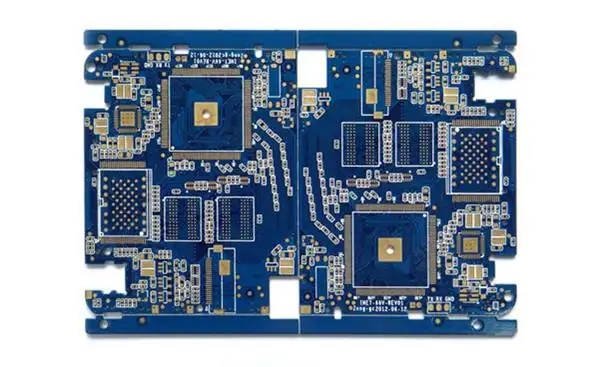
Special attention shall be paid to heat dissipation in component layout. For high-power circuits, those heating elements such as power tubes and transformers should be placed as far away as possible to facilitate heat emission. They should not be concentrated in one place, nor should high capacitors be too close to avoid premature aging of electrolyte. PCB PCB proofing
4. Wiring
Wiring principle: The knowledge of wiring is very advanced, everyone will have their own experience, but there are still some general principles. Interested friends can click:
5. Adjust and improve
After the wiring is completed, it is necessary to make some adjustments to the text, individual components, wiring and copper coating (this work should not be done too early, or it will affect the speed and cause trouble to the wiring), also for the convenience of production, debugging and maintenance.
Copper coating usually refers to filling the blank area left after wiring with a large area of copper foil. You can lay GND copper foil or VCC copper foil (but in this way, once the short circuit is easy to burn the device, it is better to ground, unless it must not be used to increase the conduction area of the power supply, so as to withstand a large current before connecting to VCC). Encapsulation usually refers to wrapping a handful of signal wires with special requirements with two ground wires (TRAC) to prevent them from being interfered or interfered by others.
If copper coating is used to replace the ground wire, attention must be paid to whether the whole ground is connected, and whether there are special requirements for the current size, flow direction, to ensure that unnecessary errors are reduced.
6. Check the network
Sometimes the network relationship of the drawn board is different from the schematic diagram due to misoperation or negligence, so it is necessary to check. Therefore, after painting, you must not rush to hand over to the plate manufacturer. You should check it first, and then carry out the follow-up work.
7. PCB PCB proofing with simulation function
After these works are completed, software simulation can also be carried out if time permits. Especially the high-frequency digital circuit, which can find some problems in advance and greatly reduce the debugging workload in the future. The circuit board assembly manufacturer explains several problems that engineers should pay attention to when designing PCB circuit boards.


Just upload Gerber files, BOM files and design files, and the KINGFORD team will provide a complete quotation within 24h.