
Professional PCB manufacturing and assembly
Building 6, Zone 3, Yuekang Road,Bao'an District, Shenzhen, China
+86-13410863085Mon.-Sat.08:00-20:00

Design Guide for High Polymer Thick Film of FPC Circuit Board
PCB manufacturers, PCB designers and PCBA manufacturers explain the design guidelines for FPC PCB polymer thick film
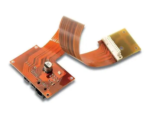
Flexible Printed Circuit Board (FPC) is referred to as "flexible Board", commonly known as FPC in the industry. It is a Flexible insulating substrate (mainly polyimide or polyester film) The printed circuit board has many advantages that the hard printed circuit board does not have. For example, it can bend, wind and fold freely. The volume of electronic products can be greatly reduced by using FPC, which is suitable for the development of electronic products in the direction of high density, miniaturization and high reliability. Therefore, FPC has been widely used in aerospace, military, mobile communications, laptops, computer peripherals, PDAs, digital cameras and other fields or products.
Because of its inherent characteristics, FPC polymer thick film (PTF) circuits have their own design criteria. Because of the screen printing technology, the design limitation is dominated by two main factors: (1) the conductivity of the selected ink and the limitation of screen printing; (2) Process used. The main limitation of the latter is the ability of circuit making. The newly developed nano particle technology may significantly improve the conductivity, which may open another window for such applications. Although they can actually deal with some specific dynamic applications, most PTF lines will not be considered for dynamic applications.
Generally speaking, the line width and spacing range with the smallest processing capacity is 375um. It is possible to use PTF ink to produce thinner lines, but the conductivity is a bigger concern for design performance.
1: Current load capacity of PTF
Silver containing polymer thick film ink can be expected to carry 25% of the current of copper wire circuit with the same width and thickness under normal conditions. However, it should be noted that when trying to maximize the line current load capacity, the hot spot on the conductor may cause rapid deterioration and cause faults.
2: Screen printed PTF resistance
Screen printing is often used to make resistors, and is usually designed with PTF circuits. If used in a design, the resistance should be kept at a minimum of one or two values to facilitate production. Generally, the resistance can be printed to a tolerance of ± 20% or so without laser trimming. After laser or mechanical trimming, the resistance can reach a smaller tolerance.
3: Considerations on endpoint design of PTF line
The design criteria of PTF circuit or gasket are similar to PCB, but the appearance of the terminal should be discussed with the manufacturer. Because the polymer thick film ink can not be directly welded, conductive adhesion can be used for surface mount component operations, and its surface mount pad design is similar to the general circuit board. PCB manufacturers, PCB designers and PCBA processors will explain the design guidelines for FPC PCB polymer thick film.


Just upload Gerber files, BOM files and design files, and the KINGFORD team will provide a complete quotation within 24h.