
Professional PCB manufacturing and assembly
Building 6, Zone 3, Yuekang Road,Bao'an District, Shenzhen, China
+86-13410863085Mon.-Sat.08:00-20:00

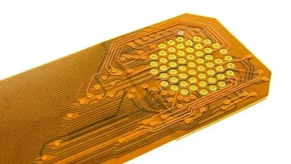
It is difficult to design irregular fingerprint module FPC?
PCB manufacturers, PCB designers and PCBA manufacturers explain to you that it is difficult to do FPC design of irregular shaped fingerprint modules? In fact, it can be done with a few moves!
The expected full fingerprint module FPC is usually a regular rectangular shape. Although most designs are indeed rectangular, many designs require irregular shaped circuit boards, which are often not easy to design.
Nowadays, the size of the fingerprint module FPC is shrinking, and the functions in the circuit board are more and more. With the improvement of the clock speed, the design becomes more and more complex. So, let's see how to deal with more complex shaped circuit boards.
Simple PCI board shapes can be easily created in most EDA Layout tools. However, when the circuit board shape needs to adapt to the complex shell with high restrictions, it is not so easy for the fingerprint module FPC designers, because the functions of these tools are different from those of mechanical CAD systems. Complex circuit boards are mainly used for explosion-proof enclosures, so they are subject to many mechanical limitations.
Rebuilding this information in EDA tools can take a long time and not be productive. Because, it is very likely that the mechanical engineer has created the shell, circuit board shape, mounting hole position and height limit required by the FPC designer of the fingerprint module.
Because there are radians and radii in the circuit board, even if the circuit board shape is not complex, the reconstruction time may be longer than expected.
However, from today's consumer electronics, you will be surprised to find that many projects try to add all the functions in a small package, which is not always rectangular. You should think of smartphones and tablets first, but there are many similar examples.
If you return the rented car, you may see that the attendant reads the car information with a hand-held scanner and then communicates with the office wirelessly. The device is also connected to a thermal printer for instant receipt printing. In fact, all these devices use rigid/flexible circuit boards, where traditional PCB circuit boards are interconnected with flexible printed circuits so that they can be folded into small spaces.
How to import the defined mechanical engineering specifications into the fingerprint module FPC design tool?
Reusing these data in mechanical drawings can eliminate duplicate work and, more importantly, human errors.
We can use DXF, IDF or ProSTEP format to import all information into PCB Layout software to solve this problem. This can not only save a lot of time, but also eliminate possible human errors. Next, we will look at these formats one by one.
DXF
DXF is a format that has been used for the longest time and is most widely used. It mainly exchanges data between mechanical and PCB design domains electronically. AutoCAD developed it in the early 1980s. This format is mainly used for two-dimensional data exchange.
Most PCB tool vendors support this format, and it does simplify data exchange. DXF import/export requires additional functionality to control which layers, different entities, and cells will be used in the exchange process.
A few years ago, 3D function began to appear in PCB tools, so a format that can transfer 3D data between machinery and PCB tools was needed. As a result, Mentor Graphics developed the IDF format, which was then widely used to transfer PCB and component information between PCB and mechanical tools.
IDF
Although the DXF format includes the size and thickness of the circuit board, the IDF format uses the X and Y positions of the component, the tag number of the component, and the Z-axis height of the component. This format greatly improves the ability to visualize PCBs in 3D views. The IDF file may also include other information about the no go zone, such as the height limits at the top and bottom of the circuit board.
The system needs to be able to control the content contained in the IDF file in a similar way to DXF parameter settings. If some components do not have height information, IDF export can add missing information during creation.
Another advantage of the IDF interface is that either party can move the components to a new location or change the board shape, and then create a different IDF file.
The disadvantage of this method is that it is necessary to re import the entire file representing changes to the circuit board and components, and in some cases, it may take a long time due to the file size.
In addition, it is difficult to determine what changes have been made through the new IDF file, especially on larger circuit boards. IDF users can eventually create custom scripts to determine these changes.
In order to better transmit 3D data, designers are looking for an improved way, STEP format came into being. STEP format can transfer the size of circuit board and component layout, but more importantly, the component is no longer a simple shape with only a height value.
STEP component model gives a detailed and complex representation of components in three-dimensional form. PCB and component information can be transferred between PCB and machinery. However, there is still no mechanism for tracking changes.
To improve STEP file exchange, we introduced ProSTEP format. This format can move the same data as IDF and STEP, and has great improvement – it can track changes, and it can also provide the function of working in the original system of the discipline and reviewing any changes after establishing the benchmark.
In addition to viewing changes, PCB and mechanical engineers can also approve all or individual component changes in layout, board shape modification. They can also suggest different board sizes or component locations. This improved communication has created an ECO (Engineering Change Order) between ECAD and the mechanical team that never existed before
Now, most ECAD and mechanical CAD systems support the use of ProSTEP format to improve communication, thereby saving a lot of time and reducing costly errors that may be caused by complex electromechanical design.
More importantly, engineers can create a complex circuit board shape with additional restrictions, and then transmit this information electronically to avoid someone mistakenly reinterpreting the size of the circuit board, thus saving time.
If you have not used these DXF, IDF, STEP or ProSTEP data formats to exchange information, you should check their usage. Consider using this electronic data exchange to stop wasting time to recreate complex board shapes. PCB manufacturers, PCB designers and PCBA manufacturers explain to you that it is difficult to do FPC design of irregular shaped fingerprint modules? In fact, it can be done with a few moves!


Just upload Gerber files, BOM files and design files, and the KINGFORD team will provide a complete quotation within 24h.