
Professional PCB manufacturing and assembly
Building 6, Zone 3, Yuekang Road,Bao'an District, Shenzhen, China
+86-13410863085Mon.-Sat.08:00-20:00

66 Common Problems in PCB High Frequency Board Design Part 3
PCB manufacturers, PCB designers and PCBA manufacturers explain 66 common problems in PCB high-frequency board design Part III
21. What aspects should the circuit board DEBUG start from?
As far as digital circuits are concerned, first determine three things in sequence:
1. Confirm that all clock signal frequencies work normally and there is no non monotonic problem on the signal edge.
2. Confirm that all power values meet the design requirements. Some systems with multiple power supplies may require some specifications for the sequence and speed of the power supplies.
3. Confirm whether the reset signal meets the specification requirements. If all these are normal, the chip should send the first cycle signal. Next, debug according to the system operation principle and bus protocol.
22. LC circuit is often used for filtering at analog power supply. But why is LC filtering worse than RC filtering sometimes?
The comparison of LC and RC filtering effects must consider whether the frequency band to be filtered and the inductance value are properly selected. Because the inductance is related to the inductance value and frequency. If the noise frequency of the power supply is low and the inductance value is not large enough, the filtering effect may not be as good as RC. However, the cost of using RC filtering is that the resistor itself will consume energy, and the efficiency is poor. In addition, attention should be paid to the power that the selected resistor can withstand.
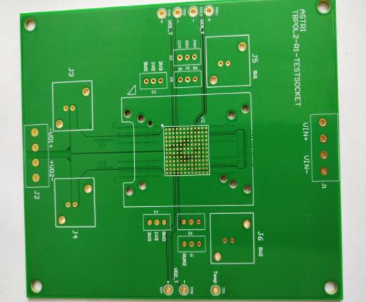
23. Explanation of the meaning of each layer of PCB high-frequency board?
Topoverlay - the name of the top device, also called topsilksscreen or topcomponentlegend, such as R1C5,
IC10. bottomoverlay -- the same with multilayer -- if you design a 4-layer board, you place a freepadorvia and define it as a multilay, then its pad will automatically appear on the four layers. If you only define it as the toplayer, then its pad will only appear on the top layer.
24. What is the method of selecting inductance and capacitance value when filtering?
The selection of inductance value shall consider not only the noise frequency to be filtered, but also the reaction ability of instantaneous current. If the LC output terminal has the opportunity to output a large current instantaneously, the inductance value is too large to hinder the speed of this large current flowing through the inductor, increasing ripple noise. The capacitance value is related to the ripple noise specification value that can be tolerated. The smaller the ripple noise value is required, the larger the capacitance value will be. The capacitor ESR/ESL will also have an impact. In addition, if the LC is placed at the output end of the switching regulation power, pay attention to the influence of the pole/zero generated by the LC on the stability of the negative feedback control circuit.
25. How to meet EMC requirements as much as possible without causing too much cost pressure?
The increased cost of EMC on PCB high-frequency board is usually due to the increase of the number of layers to enhance the shielding effect and the addition of ferritehead, choke and other high-frequency harmonic suppression devices. In addition, the shielding structure of other institutions is usually required to make the whole system pass the EMC requirements. Here are just a few ways to reduce the electromagnetic radiation effect generated by the circuit based on the design skills of the PCB high-frequency board.
Devices with slow signal slope shall be selected as far as possible to reduce the high-frequency components generated by the signal.
Pay attention to the placement of high-frequency (PCB high-frequency board) components, and do not be too close to external connectors.
Pay attention to the impedance matching of high-speed signals, the routing layer and its return current path to reduce high-frequency reflection and radiation.
Place enough and appropriate decoupling capacitors on the power supply pins of each device to mitigate the noise on the power supply layer and stratum. Pay special attention to whether the frequency response and temperature characteristics of the capacitor meet the design requirements.
The ground near the external connector can be properly separated from the stratum, and the ground near the connector can be connected to the chassis ground.
Groundguard/shuttraces can be properly used beside some signals with high speed. However, we should pay attention to the influence of guard/shuttles on the characteristic impedance of the wiring.
The power layer is 20H smaller than the formation, and H is the distance between the power layer and the formation.
26. When there are multiple digital/analog function blocks in a PCB high-frequency board, the conventional practice is to separate the digital/analog function blocks from the ground. Why?
The reason for separating D/A from ground is that the digital circuit will generate noise in the power supply and ground when switching between high and low potentials. The size of the noise is related to the speed and current of the signal. If the ground plane is not divided and the noise generated by the digital area circuit is large and the analog area circuit is very close, the analog signal will still be interfered by the ground noise even if the digital and analog signals do not intersect. That is to say, the digital analog ground undivided mode can only be used when the analog circuit area is far away from the digital circuit area that generates large noise.
27. Another method is to ensure that the digital/analog signal is laid out separately, and the digital/analog signal wiring is not crossed with each other. The whole PCB high-frequency board ground is not divided, and the digital/analog ground is connected to this ground plane. Why?
The requirement that the routing of digital and analog signals cannot cross is that the return current path of a faster digital signal will return to the source of the digital signal as far as possible along the ground near the lower part of the routing. If the routing of digital and analog signals crosses, the noise generated by the return current will appear in the analog circuit area.
28. How to consider the impedance matching problem when designing the schematic diagram of high-speed PCB high-frequency board?
When designing high-speed PCB (PCB high-frequency board) circuits, impedance matching is one of the elements of design. The impedance value has an absolute relationship with the routing method. For example, when walking on the surface layer (microstrip) or the inner layer (stripline/doublestripline), the distance from the reference layer (power layer or stratum), the routing width, PCB material, etc. will affect the characteristic impedance value of the routing. That is to say, the impedance value can be determined only after wiring. General simulation software can't take into account some discontinuous impedance wiring due to the limitation of line model or mathematical algorithm used. At this time, only some terminators (such as series resistance) can be reserved on the schematic diagram to mitigate the effect of discontinuous impedance wiring. The real fundamental solution to the problem is to avoid impedance discontinuity when wiring.
29. Where can we provide a more accurate IBIS model base?
30. When designing high-speed PCB (PCB high-frequency board), what aspects should designers consider the rules of EMC and EMI?
Generally, during EMI/EMC design, radiation and conducted should be considered at the same time. The former belongs to the part with higher frequency (>30MHz) and the latter belongs to the part with lower frequency (<30MHz). Therefore, we cannot only pay attention to the high frequency and ignore the low frequency. A good EMI/EMC design must consider the location of components, PCB stack arrangement, important online routing, and component selection at the beginning of the layout. If there is no better arrangement in advance, it will take twice the effort and increase the cost if it is resolved afterwards For example, the position of the clock generator should not be close to the external connector as much as possible, the high-speed signal should go through the inner layer as much as possible and pay attention to the continuity of the characteristic impedance matching and the reference layer to reduce reflection, the slope of the signal pushed by the device should be as small as possible to reduce the high-frequency component, and when selecting the decoupling/bypass capacitor, pay attention to whether its frequency response meets the requirements to reduce the power layer noise. In addition, note that the return path of high-frequency signal current makes the loop area as small as possible (that is, the loop impedance is as small as possible) to reduce radiation. The range of high-frequency noise can also be controlled by dividing the stratum. Finally, properly select the chassis ground between the high frequency PCB board and the housing. PCB manufacturing, PCB design and PCBA processing manufacturers will explain 66 common problems in PCB high-frequency board design Part III.


Just upload Gerber files, BOM files and design files, and the KINGFORD team will provide a complete quotation within 24h.