
Professional PCB manufacturing and assembly
Building 6, Zone 3, Yuekang Road,Bao'an District, Shenzhen, China
+86-13410863085Mon.-Sat.08:00-20:00

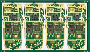
With the continuous reduction of PCB process nodes and chip sizes, the number of consumer electronic products using flip chip PCB chips to package IC devices is increasing. However, flip chip packaging and manufacturing rules have not kept up with the pace of technological development.
Therefore, a more accurate and efficient design method of I/O interface is needed, especially the design method of I/O interface PCB for flip chip design. This integrated chip package collaborative design method should allow early feasibility studies, optimize package and chip interface design, and meet strict constraints of chip and package requirements.
At present, most flip chip design companies use internal methods for flip chip planning. This method mainly uses spreadsheets to capture and store design inputs and constraints. The company develops its own script to process the data in the spreadsheet and generate instructions to guide the design and implementation. This method usually starts with a simple system, and then gradually develops into a set of complex formats and scripts as the design complexity increases.
This method has many disadvantages. First, the maintenance of this system is expensive and will reduce the productivity of PCB designers. Second, electronic forms have great limitations in design description. Third, scripts lack comprehensive ability to perform hypothesis analysis and optimize the design in terms of cost, performance and reliability. Fourthly, the system based on spreadsheets and scripts cannot accurately predict the final realization of the design.
Collaborative Design Environment
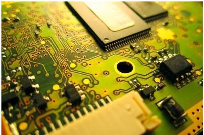
With the shrinking of bare chips and the increasing number and speed of I/O, the interface between PCB chip and package soon became the most restrictive part in the design. The package and chip with high quality and low cost can be designed in time and at the same time, which can realize successful products completely different from ordinary or faulty chips.
Therefore, an integrated chip package collaborative design system is needed, which uses industry standard database OpenAccess and can be connected with third-party packaging and interface implementation tools. This integrated design environment allows designers to view and manipulate chip and package data in a single database. Because the design database contains complete package and chip implementation data, this database can be used by both chip and package design teams.
The Tcl interface allows users to develop Tcl scripts to detect design data, generate data reports, and automate the design process. Through the use of standard interfaces such as database or LEF/DEF, data exchange can also be realized between the collaborative design environment and third-party chips and packaging implementation tools.
An efficient packaging and chip collaborative design solution must have the ability to quickly build prototypes, because packaging decisions need to be made early in the design cycle, when the design netlist and/or physical library are not ready. The accuracy of the final prediction is also important. If there is not enough precision, the design decisions made in the prototype design or planning stage may lead to difficulties in implementation, which will seriously affect the tape out time.
Conservative planning may unnecessarily increase packaging costs. Collaborative design system needs to allow users to develop a variety of PCB markets so that designers can test different packaging solutions. With this function, users can use different PCB substrates


Just upload Gerber files, BOM files and design files, and the KINGFORD team will provide a complete quotation within 24h.