
Professional PCB manufacturing and assembly
Building 6, Zone 3, Yuekang Road,Bao'an District, Shenzhen, China
+86-13410863085Mon.-Sat.08:00-20:00

The circuit board manufacturer explains how to specify the circuit board substrate?
Circuit board manufacturers, circuit board designers and PCBA manufacturers explain to you how to specify circuit board substrates?
Selecting appropriate circuit board surface treatment and optimization design is an important step to ensure excellent product performance, but is it not the end? No, you must also ensure that the circuit board factory has the specified materials, and that the factory can use the materials through UL certification. You should know that the choice of materials is diverse. Only with professional technical knowledge can we identify the selection and specification of materials.
How should the board material be specified?
It is recommended that you do not specify a specific brand or material type as far as possible, so as not to limit your choice when you finally choose the factory. The reason is that many well-known brand materials are widely used in PCB manufacturers, while some factories have several brands of materials that can meet the required material specifications. At this time, the availability and price may become the determining factors of which brand to use.
This does not mean that you cannot specify the materials you know, by no means. If you know from experience that a certain material is suitable for your product, you can list this product and add the postscript of "or equivalent material". In this way, the technicians and procurement team of PCBA processing plant will review various materials and provide you with an alternative product that can meet the functional needs without affecting the performance.
Each well-known material manufacturer classifies its products according to IPC 4101 (Specification for Base Materials of Rigid and Multilayer Printed Circuit Boards), so as to use this specification to determine performance characteristics and classify them, and defines the characteristics of the base materials in detail.

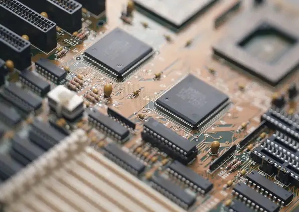
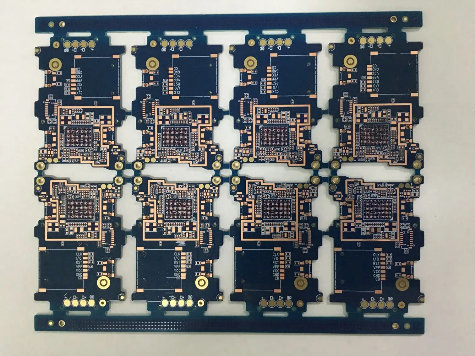
Generally, PCB substrate materials can be divided into two categories: rigid substrate materials and flexible substrate materials. In general, copper clad laminate is an important type of rigid substrate materials. It is made of Reinforeing Material, impregnated with resin adhesive, dried, cut and laminated into blanks, covered with copper foil, steel plate as a mold, and formed in a hot press under high temperature and pressure. Generally, the prepreg used for multilayer board is the semi-finished product (mostly made of glass cloth soaked with resin and dried) of copper clad laminate during the manufacturing process.
There are many ways to classify copper clad laminates. Generally, according to the different reinforcement materials of the board, it can be divided into five categories: paper base, glass fiber cloth base, composite base (CEM series), multilayer board base and special material base (ceramic, metal core base, etc.). The common paper based CCI is classified according to the different resin adhesives used for boards. There are various types of phenolic resin (XPc, XxxPC, FR - 1, FR - 2, etc.), epoxy resin (FE - 3), polyester resin, etc. Common glass fiber cloth base CCL includes epoxy resin (FR - 4, FR - 5), which is the most widely used type of glass fiber cloth base at present. In addition, there are other special resins (glass fiber cloth, polyimide fiber, non-woven fabric, etc. are added): bismaleimide modified triazine resin (BT), polyimide resin (PI), diphenylene ether resin (PPO), maleic anhydride imide styrene resin (MS), polycyanate resin, polyolefin resin, etc.
According to the classification of flame retardancy of CCL, it can be divided into flame retardant (UL94-VO, UL94-V1) and non flame retardant (UL94-HB) boards. In recent years, with more emphasis on environmental protection, a new type of bromine free CCL has been developed among flame retardant CCLs, which can be called "green flame retardant cCL". With the rapid development of electronic product technology, there are higher performance requirements for cCL. Therefore, according to the performance classification of CCL, it can be divided into general performance CCL, low dielectric constant CCL, high heat resistance CCL (L of general board is above 150 ℃), low thermal expansion coefficient CCL (generally used on packaging substrate) and other types.
With the development and continuous progress of electronic technology, new requirements are constantly put forward for PCB substrate materials, thus promoting the continuous development of copper clad foil standards. At present, the main standards of substrate materials are as follows.
① National standards At present, China's national standards for substrate materials include GB / T4721-4722 1992 and GB 4723-4725-1992. The standards for copper clad foil in Taiwan, China, China, are CNS standards, which are based on Japanese JIS standards. In 1983, like bike 2009-02-17 12:46:17 printed circuit board, also known as printed circuit board, printed circuit board, or PCB or PWB, is an important electronic component and the support of electronic components, It is the supplier of electrical connection of electronic components. Because it is made by electronic printing, it is called "printed" circuit board.
history
The inventor of the printed circuit board was PAUL EISLER, an Austrian, who adopted the printed circuit board in a radio device in 1936. In 1943, Americans used this technology in a large number of military radios. In 1948, the United States officially recognized the invention for commercial use. Since the mid 1950s, printed circuit board technology has been widely adopted.
Before the appearance of printed circuit board, the interconnection between electronic components was realized by direct connection of wires. Now, circuit breadboard only exists as an effective experimental tool; The printed circuit board has already occupied the absolute dominant position in the electronic industry.
Design
The design of printed circuit board is based on the circuit schematic diagram to realize the functions required by the circuit designer. The design of printed circuit board mainly refers to layout design, which needs to consider various factors such as the layout of external connections, the optimal layout of internal electronic components, the optimal layout of metal wiring and through-hole, electromagnetic protection, heat dissipation, etc. Excellent layout design can save production costs and achieve good circuit performance and heat dissipation. Simple layout design can be realized by hand, while complex layout design needs to be realized by computer aided design (CAD).
classification
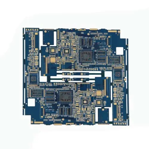
According to the number of circuit layers, it can be divided into single panel, double panel and multilayer board. The common multilayer board is generally 4-layer board or 6-layer board, and the complex multilayer board can reach more than ten layers.
Classified according to software and hardware: divided into ordinary circuit boards and flexible circuit boards.
manufacture
According to different technologies, it can be divided into two categories: elimination and addition.
eliminate
Use chemicals or machinery to remove the unnecessary parts on the blank circuit board (i.e. the circuit board with a complete piece of copper foil), and the rest is the required circuit.
Screen printing: the pre designed circuit diagram is made into a screen mask, and the unwanted circuit parts on the screen will be covered with wax or impermeable materials. Then the screen mask is placed on the blank circuit board, and the screen is oiled with a protective agent that will not be corroded. The circuit board is placed in the corrosive solution, and the parts not covered by the protective agent will be eroded away. Finally, the protective agent is cleaned.
Photosensitive board: make the pre designed circuit diagram on the light transmitting film mask (the simplest way is to use the projection film printed by the printer), similarly, print the required part into an opaque color, then apply photosensitive pigment on the blank circuit board, place the prepared film mask on the circuit board to illuminate the strong light for several minutes, remove the mask, and display the pattern on the circuit board with developer, Finally, the circuit is etched as if it were screen printed.
Engraving: use the milling machine or laser engraving machine to directly remove the unnecessary parts on the blank line.
increase
On a substrate pre coated with thin copper, cover the photoresist (D/F), develop it after ultraviolet light exposure, and expose the required area. Then use electroplating to thicken the copper thickness of the formal circuit on the circuit board to the required specification, and then coat a layer of anti etching inhibitor - metal thin tin. Finally, remove the photoresist (this process is called film removal), and then etch the copper foil layer under the photoresist.
Circuit board manufacturers, circuit board designers and PCBA manufacturers explain to you how to specify circuit board substrates?


Just upload Gerber files, BOM files and design files, and the KINGFORD team will provide a complete quotation within 24h.