
Professional PCB manufacturing and assembly
Building 6, Zone 3, Yuekang Road,Bao'an District, Shenzhen, China
+86-13410863085Mon.-Sat.08:00-20:00

The transmission rate of the high-speed PCB design wiring system is steadily accelerating, which also brings some anti-interference vulnerability. This is because the higher the transmission frequency of information, the more sensitive the signal is, and the weaker their energy is, the more vulnerable the wiring system is to interference.
Interference is everywhere. Cables and equipment will interfere with other PCB components or be seriously interfered by other interference sources, such as computer screens, mobile phones, motors, radio relay equipment, data transmission and power cables. In addition, potential eavesdroppers, network crimes and hackers are increasing, because their interception of UTP cable information transmission will cause huge damage and loss.
Especially when using high-speed data networks, the time required to intercept a large amount of information is significantly lower than the time required to intercept low-speed data transmission. The twisted pair of data twisted pair can resist external interference and crosstalk between pairs by its own twisted pair at low frequencies, but at high frequencies (especially when the frequency exceeds 250MHz), the purpose of anti-interference cannot be achieved only by twisted pair, and only shielding can resist external interference.
The cable shield acts like a Faraday shield. Interference signals will enter the shield, but not the conductor. Therefore, data transmission can operate without failure. Shielded cable has lower radiation emission than unshielded cable, thus preventing network transmission from being intercepted. Shielded network (shielded cables and components) can significantly reduce the level of electromagnetic energy radiation that may be intercepted when entering the surrounding environment.
The shielding of different interference fields mainly includes electromagnetic interference and radio frequency interference. Electromagnetic interference (EMI) is mainly low-frequency interference, and motors, fluorescent lamps and power lines are common sources of EMI. Radio frequency interference (RFI) refers to radio frequency interference, mainly high-frequency interference. Radio, television relay, radar and other wireless communication are common RF interference sources.
For electromagnetic interference resistance, braided shielding is the most effective because of its low critical resistance; For RF interference, foil shielding is the most effective. Because braided shielding depends on the change of wavelength, the gap it generates allows high-frequency signals to enter and exit the conductor freely; For the high and low frequency mixed interference field, the combination shielding mode of foil layer and woven mesh with broadband coverage function shall be adopted. Generally, the higher the mesh shielding coverage, the better the shielding effect.
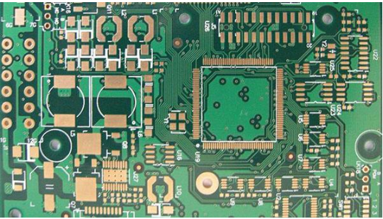
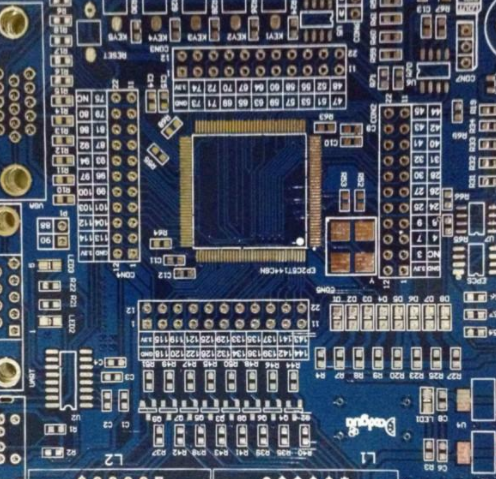
PCB design advantages
Our PCB design engineers have at least 5 years of professional PCB design experience. The company has a set of professional and rigorous PCB Design Specifications, strict Quality Standard system, and the world's advanced PCB Standard Library. Be able to quickly and accurately design the PCB required by customers according to the information provided by customers. The design we provide for customers is not just a simple LAYOUT layout and wiring work. We will consider the electrical performance for you, such as timing requirements, signal quality, signal matching scheme, signal routing topology, high-speed signal return, power ground decoupling, decoupling capacitance distribution, signal impedance and stack control, single board EMC/EMI strategy analysis, provide you with more suggestions and experience in PCB design, and create higher added value for you, So as to make the internal quality of your products higher.
The staff reserve is sufficient, and the online operation, module operation and other methods are fully used to divide tasks; Innovative morning and evening shift operation mode, flexible and diverse work allocation, ready to work overtime, weekend, night shift and other ways to shorten the delivery date. Secondly, a special project discussion group shall be established during the project design process: engineers from both sides shall "directly" communicate with each other, and business personnel shall follow up the project progress to ensure that the project progress will not be delayed by any party. In addition, combined with rich design experience, the design for manufacturability can be fully realized to minimize design duplication and rework. Truly reach the fastest delivery date in the industry.
Take advantage of the cost advantage in the mainland (because Changsha's living cost is low, especially the housing price is significantly lower than that of the first tier cities, the stability of our staff can be ensured, and our staff stability is significantly better than that of major peers), reasonably allocate resources, and effectively control costs. At the same time, we adhere to "the best design"="design quality"+"cost control"; Starting from PCB process and number of layers, under the condition of ensuring good board performance, we will provide an optimization plan throughout the process, fully evaluate the designability and manufacturability, maximize the reduction of PCB production costs for customers, balance customer needs, save time and money for customers, and achieve the perfect combination of low cost and high efficiency.


Just upload Gerber files, BOM files and design files, and the KINGFORD team will provide a complete quotation within 24h.