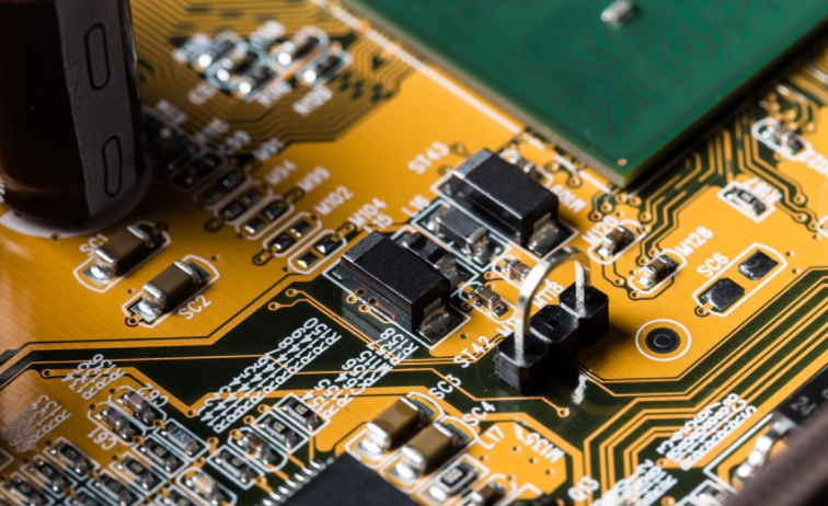
Defects of reflow soldering and BGA packaging circuits
Solder Balls
·1 PCB wire mesh hole is not connected with PCB pad, printing is not accurate, which will make solder paste dirty PCB
·2. Solder paste is exposed too much in the oxidation environment, and there is too much water in the air.
·3. The heating is inaccurate, too slow and uneven.
·4. The heating speed is too fast and the preheating interval is too long.
·5. Solder paste dries too fast.
·6. Insufficient flux activity.
·7. Too much tin powder containing small particles.
·8. Inappropriate flux fluctuation during reflux The process approval standard PCB solder ball is: when the distance between pads or printed wires is 0 13 mm, the welding ball diameter shall not exceed 0.13 mm, or there shall not be more than five welding balls in a 600 mm square area
·Bridging: Generally speaking, the reason for solder bridging is that the solder paste is too thin, including low metal or solid content in the solder paste, low thixotropy, easy extrusion of the solder paste, and too large solder paste particles. The surface tension of the flux is too small. There is too much solder paste on the bonding pad, and the reflow peak temperature is too high.
·Open: Reason:
Circuit board

·1. Insufficient solder paste.
·2. The coplanarity of component pins is not enough.
·3. The tin is not wet enough (not enough to melt, poor fluidity), and the tin paste is too thin, which will not cause tin loss.
·4. The needle absorbs tin (like rushes) or there is a connecting hole nearby. Coplanarity of pins is particularly important for fine pitch and ultra-fine pitch pin assemblies. One solution is to tin the pad in advance. Needle suction can be prevented by slowing the heating rate and heating the floor at the top. Flux with slow wetting speed and high activation temperature or solder pastes with different tin/lead ratios can also be used to slow down the melting, so as to reduce pin absorption.
Emergency Treatment of BGA Package IC Welding
Nowadays, more and more high-density, high-performance, multi pin large-scale PCB integrated circuits are packaged with ball grid array (BGA). Most of these integrated circuits are high-speed processing and high-power processors, decoders, etc. Since the pin of the BGA chip is directly located below the chip, the pin of the BGA packaged PCB chip is connected with the solder ball and the PCB pad. In addition, the thermal conduction of this chip causes the chip pin to come off the solder ball on the PCB pad, which cannot be repaired with an ordinary electric soldering iron. The best repair method is to reset the solder ball to the chip and re weld it with BGA welding station, but the general repair shop does not necessarily have this equipment. It is risky to blow weld the wafer with a hot air gun, but correct use can re weld the wafer and the circuit board. Emergency handling methods for virtual welding of BGA packaged integrated circuits under amateur conditions:
1. Solder paste must be used to remove surface oxide PCB equipment, reduce the surface tension of solder, and better integrate solder bead and pad Solder paste must be neutral and non corrosive The paste is a yellowish viscous substance Use a screwdriver to apply paste around the wafer, and then use a heating gun to heat the solder paste around the wafer at low temperature to make it drip onto the wafer (When heating, you can move the circuit board in four directions. Repeat several times, more solver paste infiltrates the solver ball)
2. Use a hot-air gun to heat the chip. Medium and high temperature gears are recommended. During heating, the air duct will blow weld wafers vertically. The air duct can move clockwise or counterclockwise at a constant speed around the circumference of the wafer substrate to make the middle silicon of the PCB chip. All other parts are heated evenly. The control of heating time is the key: if the time is too short, the solder ball will not melt and the welding will be poor; If the heating time is too long, the solder ball is easy to burst, causing short circuit between pins and damaging the chip. Recall this and observe the reaction of the solder paste. If a small amount of blue smoke is emitted, the solder paste will boil and evaporate, and the heating should be stopped immediately.
3. Press a screwdriver into the middle of the PCB chip and apply a certain pressure. The purpose is to make the tin bead contact the chip and PCB well, wait for the temperature to drop (touch the chip without heating), and then release it. After this treatment, the machine can be repaired.
The above is the explanation given by the editor of pcb circuit board company.
If you want to know more about PCBA, you can go to our company's home page to learn about it.
In addition, our company also sells various circuit boards,
High frequency circuit board and SMT chip are waiting for your presence again.


