
Professional PCB manufacturing and assembly
Building 6, Zone 3, Yuekang Road,Bao'an District, Shenzhen, China
+86-13410863085Mon.-Sat.08:00-20:00

Baking board steps for PCB processing
This PCBA board processing and baking method, large scale printed circuit boards are mostly placed in flat form, stacked 30 pieces Within 10 minutes after baking, take the PCB out of the oven and place it flat at room temperature for natural cooling Most small and medium-sized printed circuit boards are placed in a flat form, with more than 40 pieces stacked, and the number of vertical types is unlimited Remove the PCB from the oven within 10 minutes of baking Parts that are no longer used after repair do not need to be baked PCBA baking requirements: regularly check whether the material storage environment is within the specified range Personnel on duty must be trained If there is any abnormality in the baking process, the relevant technical personnel must be informed in time Anti static and thermal insulation measures must be taken when contacting materials Lead data and lead-free data need to be stored and baked separately After baking, it must be cooled to room temperature before being put on line or packaged
PCBA boards are used for most electrical equipment. This is a magic chessboard. The narrow board is filled with dense power electronic equipment to help electronic equipment complete various functions. An important part of PCBA board is baking board. What steps do we take to process PCB baking tray? What are the common questions? Let's take a closer look at the "baking steps and common conditions for PCB processing".
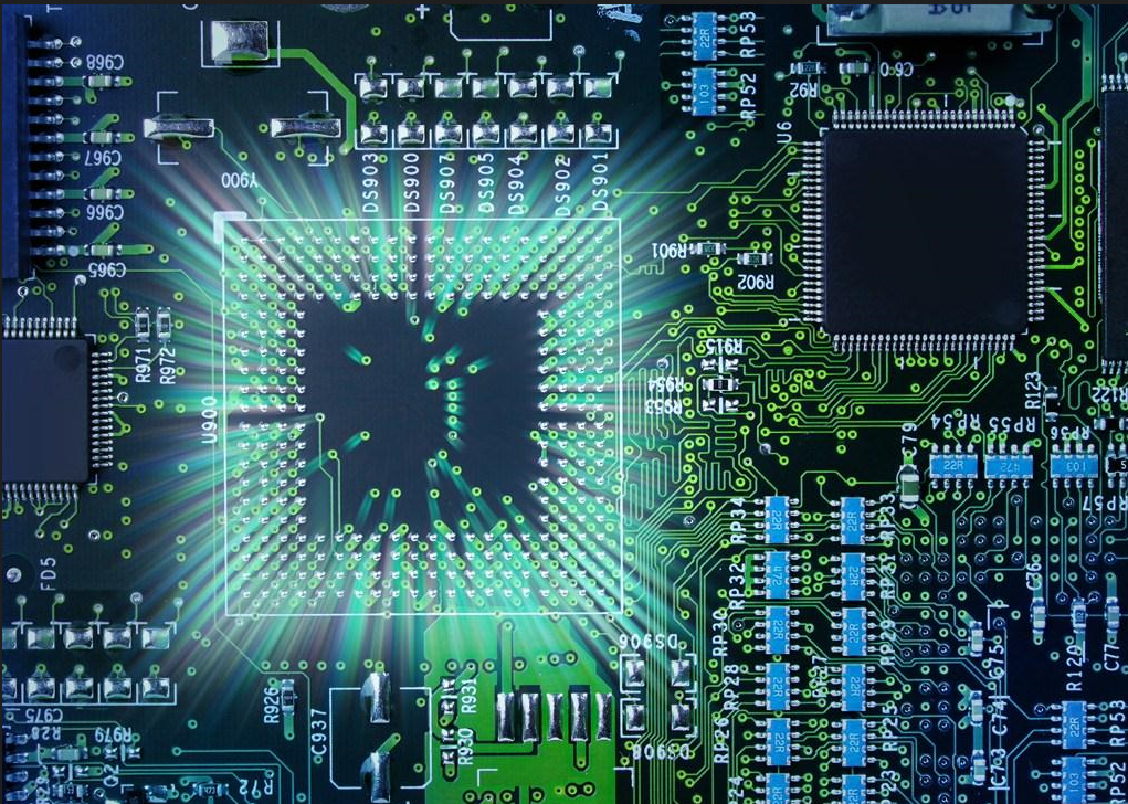
Circuit board

Before PCBA processing, there was a process that many PCB manufacturers would ignore The baking pan can remove the moisture on the PCB board and the components. After the PCB reaches a certain temperature, the flux can better combine with the components and the bonding pad The welding effect will also be greatly improved Let me introduce PCBA processing to you Baking requirements for PCBA board: the temperature is 120 ± 5 ℃, generally baking for 2 hours, and start timing when the temperature reaches the baking temperature Refer to the corresponding PCB baking specifications for specific parameters The setting of PCBA baking temperature and time, the sealing and unpacking of printed circuit boards exceed 5 days within 2 months after the manufacturing date, and the baking time is 1 hour at 120 ± 5 ℃; PCB manufacturing date is 2 to 6 months, and the temperature is 120 ± 5 ° C, baking for 2 hours; Polychlorinated biphenyls with a production date of 6 months to 1 year shall be baked at 120 ± 5 ° C for 4 hours; Baked PCBs must be treated within 5 days, while unprocessed PCBs need to be baked again. 1 It can only be put online within a few hours; Polychlorinated biphenyls that have been manufactured for more than 1 year can be baked at 120 ± 5 ° C for 4 hours and re sprayed with tin to make them online
In the process of PCBA plate processing and welding, the efficiency of flux directly affects the welding quality. What are the common welding defects in PCB processing? How to analyze and improve poor welding? The bad condition is that there are too many residues on the PCB surface after welding and the PCB is dirty. This may be due to lack of preheating or too low preheating temperature before welding, and insufficient temperature of tin furnace; The board speed is too fast; Adding antioxidant and antioxidant oil into the tin liquid; Excessive flux coating; The proportion of component feet and orifices is too large (the orifices are too large), resulting in flow accumulation; In the process of using flux, do not add thinner for a long time. If you have mastered these points, you can usually pay attention to this problem! Another kind of situation is very bad, it is easy to catch fire, which should be paid special attention! The wave furnace itself has no air knife, which will cause the flux to accumulate and drop onto the heating pipe during the heating process; Incorrect air knife angle (uneven flux distribution); There is too much glue on the PCBA board, and the glue is ignited; The circuit board moves too fast (the flux is not completely volatilized and drops into the heating tube) or too slowly (the circuit board surface is too hot); Process problems (pcba board or pcba is too close to the heating tube). Poor conditions: corrosion (green components, black solder joints). Insufficient preheating results in too much flux residue and too much harmful residue; Flux to be cleaned was used, but was not cleaned after welding. For these two reasons, what are the common conditions for handling most PCBA boards? In the process of PCBA plate processing and welding, the efficiency of flux directly affects the welding quality. Poor conditions: connection and leakage (poor insulation), and unreasonable PCB design. Shenzhen Huatao Intelligent Technology Co., Ltd. is a professional manufacturer of PCBA board design! PCB solder mask is poor in quality, easy to conduct electricity, and poor phenomena: faulty soldering, continuous soldering, solder skips, too little or uneven flux coating; Some pads or solder legs are seriously oxidized; PCB wiring is unreasonable; The foaming tube is blocked and the foaming is uneven, resulting in uneven flux coating; Improper manual tin dipping operation; The inclination of the chain is unreasonable; The wave crest is uneven. Bad phenomenon: the solder joint is too bright or not bright, which can be solved by selecting bright or matte flux; The solder used is not good. Adverse phenomena: heavy smoke and strong smell. These are things that need attention.
The problem of flux itself: using ordinary resin will produce more smoke; The activator has a lot of smoke and pungent smell; Incomplete exhaust system Adverse phenomena: tin beam technology: low preheating temperature (the flux solvent is not completely volatile); Fast board travel speed, the preheating effect is not reached; The inclination of the chain is not good, there are bubbles between the tin liquid and PCB, and tin beads are produced after the bubbles break; Improper manual tin dipping operation; Wet working environment; The board surface is wet and motion is generated; The design of the holes for the PCB to run out is unreasonable, resulting in air trapping between the PCB and the tin liquid; The design of the PCBA board is unreasonable, and the foot is too dense to cause swelling Bad phenomena: poor welding, insufficient solder joints, double wave technology, the effective components of the flux have completely volatilized when tin passes through; The circuit board moves too slowly and the preheating temperature is too high; Uneven flux coating; Solder pads and component pins are severely oxidized, resulting in poor tin corrosion; The flux coating is too little to completely wet the pad and assembly pin; Unreasonable PCBA design affects the welding of some parts Defects: 80% of PCBA solder mask peeling, peeling or blistering are caused by problems during PCB manufacturing: poor cleaning, poor solder mask, mismatch between PCB board and solder mask, etc; Tin liquid temperature or preheating temperature is too high; Too many times of welding; The PCBA plate stayed on the surface of the tin solution for a long time when the operator dipped tin The above is the poor welding phenomenon and result analysis in the welding process PCBA treatment
Precautions for PCB baking: When skin contacts PCB, you must wear heat insulation gloves. The baking time must be strictly controlled, and it cannot be too long or too short. The baked PCB must be cooled to room temperature before being put online.

Multiple prompts for embedded PCB main board
Nov 20,2022


Just upload Gerber files, BOM files and design files, and the KINGFORD team will provide a complete quotation within 24h.