
Professional PCB manufacturing and assembly
Building 6, Zone 3, Yuekang Road,Bao'an District, Shenzhen, China
+86-13410863085Mon.-Sat.08:00-20:00

Introduction to Busbar Contention in PCB Maintenance
When performing online function test on the PCB bus bar device (such as 74245), due to its bidirectional input, the test failure/output pin may be affected by other devices connected to it through the bus bar After the board under test is powered on, the bus bar device may be in the enabled state, so that its output/input pin is not in the 3-state high impedance state When bus contention occurs in the test bus equipment, the test result window In order to eliminate the impact of bus contention and pass the test of the test chip, the user must isolate the relevant bus equipment
The test results show that pins 3, 4 and 9 of the 74245 did not turn over, and the test failed. At this time, the user should check the dynamic impedance of each pin of the chip according to the pin status to determine whether any pin is short circuited to ground or has a very low resistance to ground (less than 5 ohms). From the picture in the upper right corner, you can notice that the impedance of the 11th, 16th and 17th pins to the ground is about 290 ohms, and the impedance of other output and input pins to the ground is between 17-23 ohms. The former indicates that the pin is in the logic high state, and the latter indicates that the pin is in the logic low state. The second pin passed the test and was not affected by bus contention, because its output pin can withstand the pull-down effect of the connected device.
The user must be able to distinguish whether the test failure is caused by bus contention or damaged device function. In this case, the test failed because of bus contention. In order to perform a complete test on the device, the user must isolate the relevant bus bar device and place its output pin in a high impedance state without affecting the device under test.
When the third pin of the chip is used as the output pin, it is pulled down by the connected chip and cannot be turned over. When pin 3 is used as an input pin, since the maximum drive current of QT200 is 650 mA, even if pin 3 is pulled down by other chips, QT200 can still pull pin 3 to the high potential, which can test pin 17. If the chip function is damaged, the output test of pin 17 cannot be passed at this time.
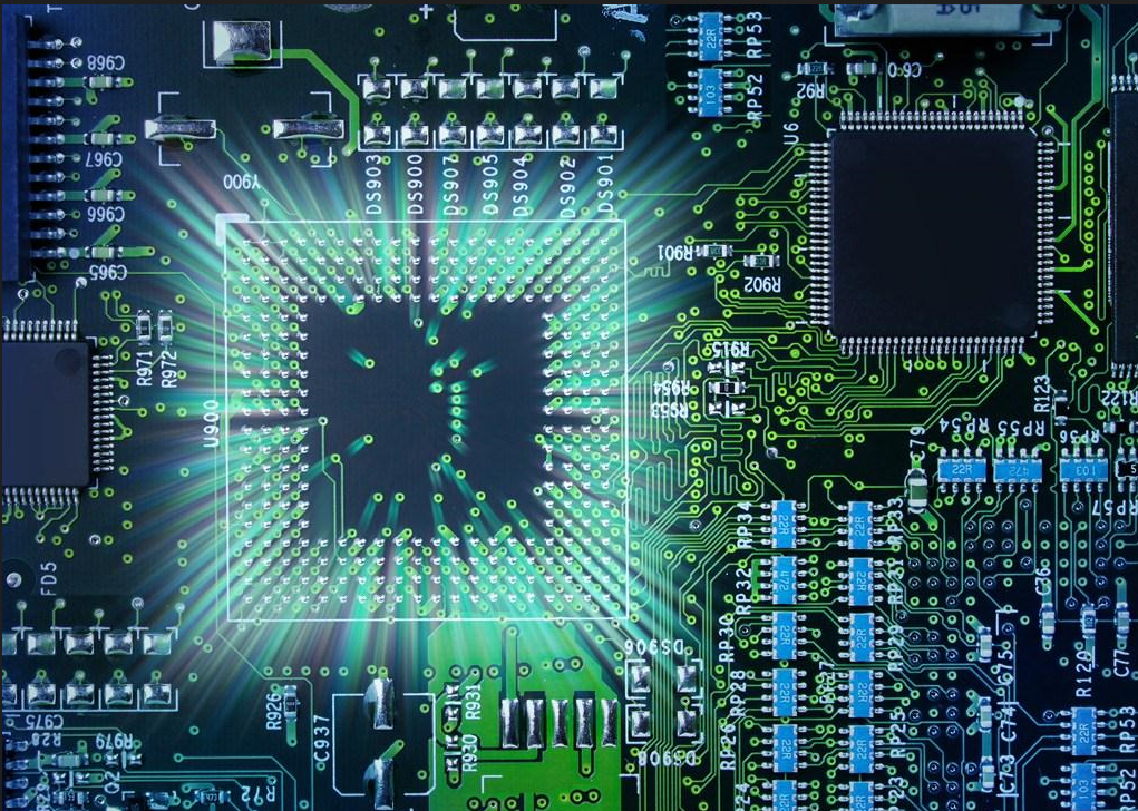
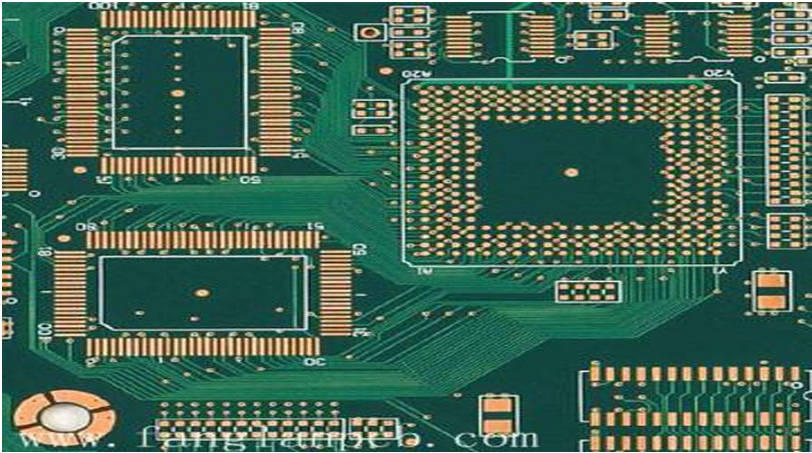
Circuit board

The actual test result shows that the 17th pin output test is passed. Obviously, the function of the chip is not damaged, but the bus is in contention
How to determine which chip causes PCB bus contention and must be isolated?
If the user has the circuit schematic diagram of the board under test, first find out all other bus bars connected to the chip under test. Generally, the busbar chips in the circuit can be divided into the following three categories:
a. The enabling terminal is connected to the output terminal of other chips;
b. Enable terminals connecting two or more busbar chips;
c. The enable terminal is directly connected to the ground or+5v power supply.
For the first type of busbar chip, set the corresponding logic level on the flying wire channel (from FC0 to FC7) of the QT200, set isolation for each enabling terminal, and then connect to these enabling terminals respectively; For the second type of busbar chip, only one isolation channel is provided, which is connected to the enable terminal of one of the chips; For the third type of busbar chip, since the isolation channel cannot realize reverse drive on its enabling terminal, the isolation setting cannot be directly executed. The general processing principle is to first set the first two kinds of busbar chips to see whether the test results of the tested chips are satisfactory (that is, the quality of the chips can be judged from the results). If satisfied, the isolation of the third type of busbar chips is not considered; If still unsatisfied, take measures to isolate Class 3 busbar chips. Generally, the secant method is used to disconnect the enable terminal from the grounding or+5v power supply and then isolate it.
After setting the isolation point, retest the chip. If the test passes, remove the set isolation channels one by one and retest. When the test fails, the bus chip whose isolation setting is deleted is the chip that generates bus contention. Reconnect the isolation channel of the chip, and continue to check other unidentified bus chips according to the above method. Until finally, find all the bus chips that need to be isolated (in board learning mode, start the notepad to record which chips need to be isolated to test which bus chips, which will be very helpful in repairing damaged circuit boards).
If the user does not have a circuit diagram, he can use the scanning test in the QSM/VI test method to find out other bus chips connected to the chip under test. The specific method is: directly enter the interactive QSM/VI test window from the ICFT test mode, customize the name of the chip to be tested, set the number of pins to 40, the measurement frequency to 312Hz, use the QT200 cable for circuit tracking (there are two 20 pin clamps), connect the clamp 1 to the bus bar chip for functional test (the first pin of the clamp faces the first pin of the chip), Connect the clamp 2 to any other bus chip on the test board, and then start scanning the test. If there is a connection between the two chips, it will be displayed in a window on the screen. Among them, pins 1-20 represent chips connected to fixture 1, and pins 21-40 represent chips connected to fixture 2. If the 5th pin and 35th pin in the window are marked with L1 symbol, it means that the 5th pin of the first chip is connected to the 15th pin of the second chip.
How to use the digital oscilloscope function of the system to judge the quality of busbar equipment?
When testing the bus bar equipment, if the quality of the equipment cannot be judged through isolation, the latest function of the system's digital oscilloscope (DSO) can be used for testing. The basic operation methods are as follows:
Re solder the crystals welded on the test PCB to make the circuit board have normal clock operation.
Connect the test probe to the appropriate channel (note that the selected probe channel varies depending on the version of the system software)
Press the DSO key on the test window toolbar to start the digital oscilloscope mode.
Open the power PCB of the equipment under test
Connect the probes to different pins of the tested busbar equipment in turn, and you can see the actual signals of the tested pins on the screen. If the signal changes from high to low, the pin functions normally. If the signal potential is fixed between 2v and 1.8v, pay special attention to the pin. This may be because the function of the pin is damaged, or the pin is an output pin in an open circuit state. At this time, 7404 chip near the crystal can be detected, because the chip is usually used for clock circuit. Use the probe to test the output pin of 7404, there should be a waveform signal. If not, check whether the power supply of the PCB under test is normal and whether the crystal is damaged. Note that 100K impedance should be selected when the oscilloscope detects the clock signal to avoid the impact on the crystal oscillator circuit.
In order to detect whether the pin is in the floating state, the impedance of the oscilloscope can be selected as 10K If the pin is inserted floating (its impedance is greater than 1 megaohm), then when the probe contacts the pin, the 10K impedance pulls the pin to the low level If the pin does not remain floating but has a fixed level, the probe will not pull it down From this, the actual PCB pin can be judged
The above is the explanation given by the editor of pcb circuit board company.
If you want to know more about PCBA, you can go to our company's home page to learn about it.
In addition, our company also sells various circuit boards,
High frequency circuit board and SMT chip are waiting for your presence again.
Forming Process of PCBA Integrated Circuit Lead
Nov 20,2022


Just upload Gerber files, BOM files and design files, and the KINGFORD team will provide a complete quotation within 24h.