
Professional PCB manufacturing and assembly
Building 6, Zone 3, Yuekang Road,Bao'an District, Shenzhen, China
+86-13410863085Mon.-Sat.08:00-20:00

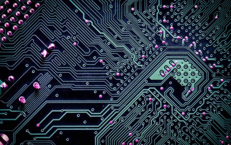
PCB inner layer production process and skills
With 3 layers of PCB
Or more commonly referred to as multilayer PCB. Traditional double-sided boards are densely assembled with matching parts. It is impossible to place so many components and a large number of circuits derived from them on a limited circuit board surface, and there are multiple layers. The development of PCB.
Most of the original four layer PCB boards are upgraded to six layer PCB boards Of course, due to high-density assembly of advanced multilayer PCB, circuit boards are also being added This chapter discusses the multilayer PCB board
Production process
There are 3 processes according to different products
A. Printing and Etching
Sending - aligning holes - copper surface treatment - image transmission - etching - stripping
B. Punching after etching
Sending - copper surface treatment - image transmission - etching - stripping film - tool hole
C. Drilling and panel
Sending - drilling - through-hole - electroplating - image transmission - etching - stripping
Question
The sending data is to cut the base plate according to the BOM according to the working size planned in the pre production design. This is a very simple step, but the following points must be noted:
A. The cutting method will affect the cutting size
B. Considering the influence of edges and fillets on the yield process of image transmission
Circuit board

C. The direction should be the same, that is, the warp direction is opposite to the warp direction, and the latitude direction is the same as the weft direction
D. Consideration of baking dimensional stability before the next process
Copper surface treatment
In the PCB manufacturing process, no matter what step, the cleaning and roughening effect of the copper surface is related to the success or failure of the next process, so it seems very simple, but in fact, there is a lot of knowledge
A. The processes requiring copper surface treatment are as follows
a. Dry film pressing
b. Before inner layer oxidation treatment
c. After drilling
d. Before chemical copper
e. Before copper plating
f. Before green paint
g. Before tin spraying (or other pad processing program)
h. Gold finger before nickel plating
This section discusses the best pipeline for processing a.c.f.g and other processes (the rest are part of process automation and do not need to be independent)
B. Handling method
Current copper surface treatment methods can be divided into three types:
a. Brush
b. Sand blasting (pumice)
c. Chemical Methods (Microbiology)
The following is an introduction to the three methods
Galloping
A. The effective length of the brush wheel must be used evenly, otherwise it is easy to cause uneven height of the brush wheel surface
b. Brush mark test must be carried out to determine the advantages of brush depth and uniformity
a. Low cost
b. Simple manufacturing technology and poor flexibility
A. Thin circuit board is not easy to realize
b. Base material elongation, not applicable to inner plate
c. When the brush mark is deep, it is easy to cause D/F adhesion and penetration
d. Possibility of residual glue
Sandblasting
Advantages of using fine stone (usually called pumice) from different data as grinding data:
a. The surface roughness and uniformity are better than that of brush coating
b. Better dimensional stability
c. It can be used for sheet and thin wire. Disadvantages:
a. Pumice is easy to adhere to the surface
b. It is not easy to maintain the machine
Chemical method (micro etching method)
Image transmission
Printing methods
The above is the explanation given by the editor of pcb circuit board company.
If you want to know more about PCBA, you can go to our company's home page to learn about it.
In addition, our company also sells various circuit boards,
High frequency circuit board and SMT chip are waiting for your presence again.


Just upload Gerber files, BOM files and design files, and the KINGFORD team will provide a complete quotation within 24h.