
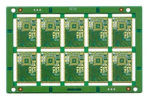
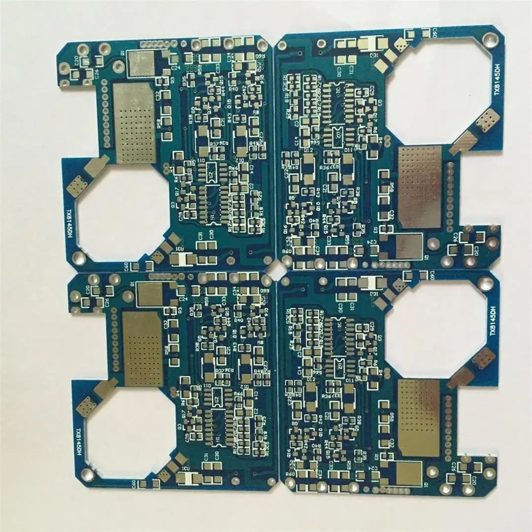
Professional PCB manufacturing and assembly
Building 6, Zone 3, Yuekang Road,Bao'an District, Shenzhen, China
+86-13410863085Mon.-Sat.08:00-20:00

Inspection before PCB dropping and post processing flow of PCB design
PCB manufacturing, PCB design and PCBA processing manufacturers will explain the process of PCB pre drop inspection and PCB design post processing
What are the inspection items before PCB dropping? Today we will explain to you:
1、 Internal QA review
1. After receiving the launch process, QA in the group first confirms that the designer has carried out full self inspection. If not, it returns to the process and requires the designer to resubmit the process after completion.
2. Review and record review results, handling opinions, etc. If the review fails, it will be returned to the designer.
3. The internal QA review comments shall be filled in the board design review record database at the same time.
2、 Check for short circuit and open circuit
Be careful when dealing with single point grounding, plane layer hollowing, and modifying the thermal pad of the pad pattern pad, and write the processing results into the ground source division of the design file, which is conducive to self inspection, QA review, and the next board modification.
2. When the electrical stratum of P software is negatively divided, it must be carefully checked. The inspection method is as follows: set PLANENET assigned to the same layer to different colors. If a cross split occurs, you need to edit the PLANETHERMAL attribute of the pads and vias in the cross region so that they do not generate a disk in the region, and then ensure their connectivity through wiring.
3. No wiring area must be added where there are windows or slots to prevent open circuit. The prohibited area defined in the structural element diagram shall also meet the requirements.
4. The correct DRC must be set and all DRC checks must be turned on.
The above is the content of the inspection items before PCB placement, do you know?
What are the post processing procedures and work steps for PCB design?
The post processing of PCB design is very much and complex. What are the post processing processes and work steps of PCB design?
1. DRC inspection: that is, design rule inspection. It focuses on avoiding major design defects such as open circuit and short circuit through checklists and reports, and follows PCB design quality control processes and methods at the same time.
2. DFM inspection: After the PCB design is completed, whether it is the processing of bare PCB boards or the chip assembly processing of PCBA support boards, it is necessary to check the processing related design with the help of relevant inspection tool software or Checklist.
3. ICT design: some PCB boards will undergo ICT test in batch processing and production, and such PCB boards need to add ICT test points in the design phase.
4. Screen printing adjustment: clear and accurate screen printing design can improve the convenience and accuracy of subsequent testing, assembly and processing of circuit boards.
5. Drill layer marking: The information marked on the Drill layer is the processing requirement drawing provided to the PE of the PCB processing factory. It needs to follow the industry specifications to ensure the accuracy and completeness of the drill processing information.
6. PCB design document output: the final document of PCB design needs to be output as different types of packaging documents according to the specifications for subsequent testing, processing and assembly.
7. CAM350 inspection: CAM files output from PCB design to PCB processing plant need to be reviewed by using CAM350 software before board placement.
PCB manufacturing, PCB design and PCBA processing manufacturers will explain the process of pre PCB inspection and post PCB design.


Just upload Gerber files, BOM files and design files, and the KINGFORD team will provide a complete quotation within 24h.