
Professional PCB manufacturing and assembly
Building 6, Zone 3, Yuekang Road,Bao'an District, Shenzhen, China
+86-13410863085Mon.-Sat.08:00-20:00

Several PCB design principles that PCB manufacturers must know
1. Layout
First, consider PCB size. When the PCB size is too large, the printed line is long, the impedance increases, the noise resistance decreases, and the cost increases; If it is too small, the heat dissipation is poor, and adjacent lines are vulnerable to interference. After determining the PCB size Then determine the position of special components. Finally, all components of the circuit are arranged according to the functional unit of the circuit.
The following principles shall be observed when determining the location of special components:
(1) Shorten the connection between high-frequency components as much as possible, and try to reduce their distribution parameters and mutual electromagnetic interference. Components susceptible to interference shall not be too close to each other, and input and output components shall be as far away as possible.
(2) There may be high potential difference between some components or wires. The distance between them should be increased to avoid accidental short circuit caused by discharge. Components with high voltage shall be arranged at places where it is not easy to reach during commissioning.
(3) The position occupied by the positioning hole of the printing plate and the fixing bracket shall be reserved.
According to the functional unit of the circuit, the layout of all components of the circuit shall comply with the following principles:
(1) Arrange the position of each functional circuit unit according to the circuit flow, so that the layout is convenient for signal flow and the signal is kept in the same direction as far as possible.
(2) Take the core components of each functional circuit as the center, and arrange around it. The components and parts shall be evenly, orderly and compactly arranged on the PCB, and the leads and connections between components and parts shall be minimized and shortened.
(3) For circuits operating at high frequencies, the distribution parameters between components should be considered. For general circuits, components shall be arranged in parallel as far as possible. In this way, it is not only beautiful, but also easy to assemble and weld, and easy to mass produce.
(4) Components located at the edge of the circuit board are generally not less than 2mm away from the edge of the circuit board. The optimal shape of the circuit board is rectangle. The length width ratio is 3:2 to 4:3. When the size of the circuit board is larger than 200x150mm, the mechanical strength of the circuit board shall be considered.
2. Wiring
The principle of wiring is as follows:
(1) The wires used at the input and output terminals shall not be parallel to each other. It is better to add ground wire between lines to avoid feedback coupling.
(2) The minimum width of the printed photographic wire is mainly determined by the adhesion strength between the wire and the insulating substrate and the current value flowing through them.
(3) The corners of printed wires are generally circular arcs, while right angles or included angles will affect the electrical performance in high-frequency circuits. In addition, try to avoid using large area copper foil, otherwise When heated for a long time, the copper foil is easy to expand and fall off. When a large area of copper foil must be used, it is better to use grid shape, which is conducive to eliminating volatile gases generated by the heating of the adhesive between the copper foil and the substrate.
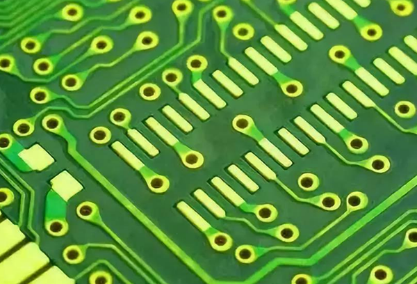
3. Pad
The pad center hole (in-line device) is slightly larger than the device lead diameter. If the pad is too large, it is easy to form faulty soldering. The outer diameter D of the pad is generally not less than (d+1.2) mm, where d is the lead hole diameter. For high-density digital circuits, the minimum diameter of the pad can be (d+1.0) mm.
Anti interference measures for PCB and circuit:
The anti-interference design of printed circuit board is closely related to the specific circuit. Here, we will explain some common measures for PCB anti-interference design.
1. Power cord design
According to the current of the printed circuit board, try to rent the width of the power line to reduce the loop resistance. At the same time, make the direction of power line and ground wire consistent with the direction of data transmission, which helps to enhance the anti noise ability.
2. Section design
The principle of ground wire design is:
(1) Separated digitally from analog. If there are both logic circuits and linear circuits on the circuit board, they should be separated as far as possible. The grounding of low-frequency circuit shall adopt single point parallel grounding as far as possible. If the actual wiring is difficult, part of the circuit can be connected in series and then connected to the ground in parallel. High frequency circuit should adopt multipoint series grounding, and the ground wire should be short and leased. The grid shaped large area foil should be used around the high frequency components as much as possible. Xinyingda embedded Internet of Things intelligent hardware Penguin needs to be demonic Wuwuba Jiuling.
(2) The grounding wire shall be thickened as much as possible. If the ground wire is sewn, the ground potential will change with the change of current, which will reduce the noise resistance. Therefore, the grounding wire should be thickened so that it can pass three times the allowable current on the printed board. If possible, the grounding wire should be more than 2~3mm.
(3) The grounding wire forms a closed loop. For printed circuit board composed of digital circuits only, the grounding circuit of the printed circuit board is arranged into a group loop, which can improve the anti noise ability.
4. Decoupling capacitor configuration
One of the common ways of PCB design is to configure appropriate decoupling capacitors in each key part of the PCB. The general configuration principle of decoupling capacitor is:
(1) The power input terminal is connected with 10~100uf electrolytic capacitor. If possible, it is better to connect the cable above 100uF.
(2) In principle, each integrated circuit chip should be equipped with a ceramic chip capacitor of 0.01uf-0.1uf. If the gap between printed boards is insufficient, a capacitor of 1-10pF can be arranged every 4-8 chips.
(3) For devices with weak noise resistance and large power supply change during shutdown, such as RAM and ROM memory devices, decoupling capacitors should be directly connected between the power line and ground wire of the chip.
5. Through hole design
In high-speed PCB design, seemingly simple vias often bring great negative effects to circuit design. In order to reduce the adverse effects caused by the parasitic effects of vias, we can try our best to
(1) Considering the cost and signal quality, the reasonable size of vias is selected. For example, for the 6-10 layer memory module PCB design, it is better to select 10/20mil (drilling/pad) vias. For some high-density small size boards, you can also try to use 8/18Mil vias. Under the current technical conditions, it is difficult to use smaller vias (when the depth of the hole exceeds 6 times of the drilling diameter, it is impossible to ensure that the hole wall can be uniformly copper plated); For the via of power supply or ground wire, the larger size can be considered to reduce the impedance
(2) The signal wiring on the PCB shall not change layers as much as possible, that is, unnecessary vias shall not be used as much as possible
(3) The pins of power supply and ground shall be punched nearby, and the lead between the via and pin shall be as short as possible
(4) Place some grounded vias near the vias for signal layer change, so as to provide the nearest circuit for the signal. You can even place a large number of redundant grounding vias on the PCB
6. Some experience in reducing noise and electromagnetic interference
(1) If you can use low-speed chips, you don't need high-speed chips. High speed chips are used in key places
(2) The method of stringing a resistance can be used to reduce the jump rate of the upper and lower edges of the control circuit.
(3) Try to provide some form of damping for relays, such as RC setting current damping
(4) Use the clock with the lowest frequency meeting the system requirements.
(5) The clock shall be close to the device using the clock as much as possible. The shell of the quartz crystal oscillator shall be grounded. The clock area shall be circled with a ground wire. The clock wire shall be as short as possible. The wire shall not be routed under the quartz crystal and the noise sensitive device. The clock, bus and chip selection signal shall be far away from the I/O line and connector. The clock line perpendicular to the I/O line has less interference than the parallel I/O line
(6) The unused gate circuit input terminal shall not be suspended, the unused op amp positive input terminal shall be grounded, and the negative input terminal shall be connected to the output terminal
PCB manufacturers, PCB designers, and PCBA manufacturers explain several PCB design principles that PCB manufacturers must know.


Just upload Gerber files, BOM files and design files, and the KINGFORD team will provide a complete quotation within 24h.