
Professional PCB manufacturing and assembly
Building 6, Zone 3, Yuekang Road,Bao'an District, Shenzhen, China
+86-13410863085Mon.-Sat.08:00-20:00


Analyze the function of copper laying in PCB production
If the PCB has multiple "causes", such as S grounding, AGND, GND, etc, The main "ground" in the jet<1 href="/tw/pcb board. html" target="_blank">PCB boards are recorded separately according to the board position This is contact At the same time, the Earth
Copper is widely used for several reasons
1.) EMC. It is used for large area of land or air supply, with masks, and some special areas, such as PGND protection
2) PCB-Required process. The copper fuse PCB is located on the floor with small wiring to avoid the influence of electroplating and lamination deformation
3) Requires a mark of integrity. The circuit provides a complete range of high-frequency digital signals and reduces wiring in the DC network Of course, there are also reasons for air heat loss and installation of special equipment There are many reasons for bronze coating
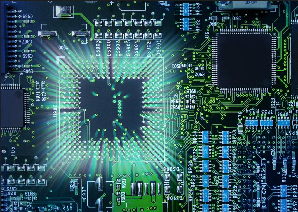
PCB board

a. EMC. It is used for large area of land or air supply, with masks, and some special areas, such as PGND protection
b. PCB processor required The copper fuse PCB is located on the floor with small wiring to avoid the influence of electroplating and lamination deformation
c. Signal integrity requirements provide a complete return path for high-frequency digital signals and reduce the wiring of DC network Of course, there are also some reasons, such as heat dissipation, copper required for installation of special devices, etc
1. One of the main advantages of copper pavement is to reduce soil resistance (many so-called antifouling agents are also due to the reduction of soil resistance). Since digital circuits contain a lot of peak currents, it is necessary to further reduce the grounding impedance It is generally believed that circuits containing digital devices need a larger grounding area For analog circuits, the grounding loop formed by copper coating will lead to electromagnetic coupling Interference that exceeds the gain (excluding high-frequency circuits). Therefore, not all circuits need ordinal coupler (by the way: coupler mesh has better shielding performance than the entire block)
2. The importance of copper circuit in the circuit is reflected in the following aspects: 1. Because the copper wire path is connected to the ground wire, the loop area can be reduced 2. Laying a large area of copper is equivalent to reducing the resistance of the grounding wire and reducing the voltage drop between these two points That is to say, whether it is digital grounding or analog grounding, copper needs to be added to enhance anti-interference capability. At high frequencies, it is necessary to separate digital grounding from analog grounding, lay the copper sheet, and then connect them to a point Before connection, this single point can be wound around the magnetic ring with a wire for several times However, if the frequency is not too high or the equipment is in good working condition, it can be quiet The crystal oscillator can be regarded as the high-frequency radiation source in the circuit, disperse copper, and then polish the crystal oscillator shell
3. What is the difference between copper block and power grid? Detailed analysis has 3 functions. 1. Aesthetic 2. Anti noise 3. Reduce high-frequency interference (due to circuit board) according to wiring standards: why should the power supply and ground plane be as wide as possible? Add grid? Oh, is this against the principle? This is even wrong when it comes to high frequencies. If high-frequency wiring is taboo, then sharp effects are also taboo. If the power plane exceeds 90 degrees, many problems will occur. In fact, why is the whole process required? Check whether the type of hand drawn solder is almost inconsistent. If you see such a picture, it must be gone. At that time, the reason was the installation of wave soldering technology. He had to heat the table locally. Of course, if the heat transfer coefficient is different, all the copper will disperse, and the circuit board will rise. When it rises, the circuit board will have problems. The tip pin is located on the top steel cover (this also requires a process). It is easy to make mistakes, and the frequency of brushing teeth is increasing. In fact, this method has its disadvantages. The current etching process makes the film easy to adhere. In future strong acid projects, these points may not be corroded and there are many residues., But if the chessboard is broken, the fragments on it will be eaten by the chessboard! Do you know why you need to draw from this angle? Of course, some surface devices are not classified. In terms of product consistency, there are two possible scenarios. 1. The corrosion process is very good. 2. Do not use wave soldering, but use reflow soldering, but in this case, the overall investment in the assembly line will be 3-5 times higher.


Just upload Gerber files, BOM files and design files, and the KINGFORD team will provide a complete quotation within 24h.