
Professional PCB manufacturing and assembly
Building 6, Zone 3, Yuekang Road,Bao'an District, Shenzhen, China
+86-13410863085Mon.-Sat.08:00-20:00


Laser Technology for HDI PCB
With the rapid development of microelectronics technology, the wide application of large-scale and ultra large scale integrated circuits, and the progress of micro assembly technology, this HDI PCB manufacturing is moving towards the direction of layering and multi-function. PCB circuit boards have thin and microporous graphics lines and narrow spacing The mechanical drilling technology used in processing can no longer meet the requirements, and a new micro hole processing method, namely laser drilling technology, has been rapidly developed
HDI PCB Laser Hole Forming Principle
Laser is a powerful beam, which is stimulated externally to add energy. Infrared and visible light have thermal energy, and ultraviolet light has light energy. When this type of light shines on the workpiece surface, there will be three phenomena: reflection, absorption and penetration.
The laser spot is impacted on the substrate by another optical element. There are multiple synthesis modes and three reactions with the illumination point.

The main function of laser drilling is to quickly remove the substrate to be processed. It mainly depends on photothermal ablation and photochemical ablation or so-called ablation.
Photothermal ablation: the principle of the hole formed by the data being processed, which absorbs high-energy lasers and heats, melts and evaporates in a very short time. Under the action of high energy, the carbon black residue formed on the pore wall must be removed before pore formation.
2. Photochemical ablation: refers to the high photon energy in the ultraviolet region exceeds 2eV electron volts. Results of high-energy photons with laser wavelengths exceeding 400 nm. This high-energy photon destroys the long molecular chain of the organic material and becomes smaller particles, but its energy is larger than the original molecule and forced to escape. In addition, the substrate material is quickly removed and formed micropores under external extrusion.
This process does not contain boiling and carbonization will not occur. In this case, pre porous cleaning is very simple.
These are the basic principles of laser drilling. At present, there are two most commonly used laser drilling methods: the laser used for drilling on PCB is mainly composed of RF excited CO2 gas laser and UV solid-state Nd: YAG laser.
3. Regarding the absorbance of the substrate: the success rate of laser is directly related to the absorbance of the substrate. PCB is a combination of copper foil, glass cloth and resin. The absorbance of these three materials varies with wavelength, but the absorbance of copper foil and glass cloth under ultraviolet light is 0.3m. The area below m has a high absorptivity, but it drops sharply after entering the visible light and infrared light. The organic resin data maintains a fairly high absorption in all three spectral segments. This is the characteristic of resin materials and the basis for the popularization of laser drilling technology.
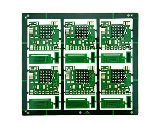
HDI PCB
Different HDI-PCB processes for CO2 laser hole formation
There are two main methods for CO2 laser drilling: direct drilling and mask drilling. The so-called direct perforation technology is to modulate the diameter of the laser beam to the same diameter as the hole on the printed circuit board through the main control system of the device, and directly process the hole on the dielectric surface without using copper foil. The coating mask process uses a special mask to coat the surface of the printed circuit board, and uses a conventional process to remove copper foil from the hole surface through exposure/development/etching. These holes are then irradiated with a laser beam larger than the aperture to remove the exposed dielectric layer resin. The following are described respectively:
1. Copper window opening pipe:
First, press a layer of RCC coated resin copper foil on the inner plate. The window is made by photochemistry, then the resin is etched to expose it, and then the substrate in the window is ablated by laser to form a micro blind hole:
When the beam is enhanced, it reaches two groups of galvanometer type micro reflection scanners through the aperture, and these scanners are vertically aligned with the positive F lens once. Arrive at the tube area where the excitation table can be made, and then burn the micro blind holes one by one.
Once the fast electron beam is positioned in a tubular area about one inch square, the 0.15mm blind hole can be punched three times. The pulse width of the first gun is about 15mS, providing energy for hole formation. After that, you can use a spray gun to clean the residue at the bottom of the hole wall and correct the hole.
The 45 degree overall view of SEM cross section and 0.15mm micro blind hole has good laser energy control. This window opening process is used as a background target. When large typesetting or second-order blind holes are not often required, they are difficult to align.
2. Window opening method:
The diameter of the hole formed by the former process is the same as that of the open copper window. A minor error in operation may cause the open window to deviate from its position, resulting in the misplacement of the blind hole position and the center of the base pad. The deviation of the copper window may be due to the expansion and contraction of the matrix data and the deformation of the negative film used for image transmission. In this case, the process of opening the large copper window is to expand the diameter of the copper window to 0.05mm larger than the diameter of the base cushion. In general, the size of the hole is determined by the size of the hole. When the hole is 0.15 mm, the diameter of the base pad should be about 0.25 mm, and the diameter of the large window should be 0.30 mm. Then, laser drilling can be carried out to precisely align the burnt position with the micro blind hole of the substrate. Its main feature is that it has a large degree of freedom of choice. When drilling laser holes, you can choose to drill according to the program of the inner base cushion. This effectively avoids the dislocation caused by the same diameter of the copper window and the hole, thus preventing the laser point from pointing to the front window and causing many incomplete half holes or residual holes on a large number of slabs.
3. HDI PCB resin surface direct pore forming process
There are several laser drilling methods for drilling with HDI PCB laser:
A. The inner layer of the substrate is coated with resin coated copper foil, and then all the copper foils are etched. The holes can be directly formed on the exposed resin surface by CO2 laser, and then the holes can be further treated according to the electroplating process.
B. The base plate is a similar process, using FR-4 semi solidified plate and copper foil instead of resin coated copper foil.
C. The copper foil is then laminated with coated photosensitive resin.
D. It is made of dry film as dielectric layer and copper foil pressing process.
E. The process of coating other types of hot films with copper foil.
4. Direct ablation of ultra-thin copper foil
After pressing the resin copper foil on both sides of the inner core plate, the thickness of the 17m copper foil is reduced to 5min by the "semi etching" method, and then black oxidation treatment is carried out to form holes by CO2 laser.
The basic principle is that the oxidized black surface will strongly absorb light, so that under the premise of adding CO2 laser beam energy, it can directly drill holes on the ultra-thin copper foil and resin surface. However, the most difficult thing is to ensure that the "semi etching method" can obtain a copper layer of uniform thickness, so special attention should be paid to its manufacturing. Of course, the copper back can tear the data. Copper foil is equivalent to a book of about 5 microns.
According to this type of sheet processing, the following main aspects are adopted in this process:
This mainly sets strict quality and technological standards for the data suppliers to ensure that the thickness difference of the dielectric layer is 510mM to M. Because only the uniformity of the dielectric thickness of the resin coated copper foil can be guaranteed, the accuracy of the weld bead and the cleanliness of the hole bottom can be guaranteed under the same laser energy. At the same time, in the subsequent operation, the best process conditions shall be used to remove the drilling dirt to ensure that the bottom of the blind hole is clean and free of residues after laser drilling. It has a good effect on the quality of blind hole electroless plating and electroplating.
Nd: YAG laser drilling HDI-PCB process
YAG is neodymium and yttrium aluminum garnet. An ultraviolet laser emitted by two solid crystals. Recently, the most commonly used laser beams excited by diode pulses can be used to manufacture effective laser sealing systems without water cooling. The third harmonic wave length of the laser is 355 nm. The fourth harmonic wave length is 266 nm. The wavelength is modulated by an optical crystal.
The biggest feature of this laser drilling is ultraviolet light. In the spectral area, although the copper foil and glass fiber composed of copper clad plate absorb strongly in the ultraviolet region, the energy of these laser points is very small. They can strongly penetrate the copper foil and glass cloth and directly form holes. Due to the small heat of the above types of lasers, carbon slag will not be generated after CO2 laser drilling, providing a good surface for subsequent hole wall operations.
YAG laser technology processes logo blind holes and through holes on various materials. It drills holes in the polyimide copper clad laminate with a minimum diameter of 25 microns. From the cost analysis, the most economical diameter used is 25125 microns. The drilling speed is 10000 holes/minute. Direct laser punching with a maximum aperture of 50 microns can be used. The inner surface of the formed hole is clean, non carbonized and easy to electroplating. It can also drill holes in PTFE CCL with a minimum diameter of 25 microns and the most economical diameter of 25125 microns. The drilling speed is 4500 holes/minute. No window pre etching is required. The hole is clean without special treatment requirements. There are other materials, such as forming hole processing. The following procedure is available for specific processing: 1. According to the two laser drilling speeds, two combined processes are adopted
The basic operation method is to first ablate the copper foil on the hole bit surface with YAG, and then directly ablate the resin with CO2 laser faster than YAG drilling.
Actual quality problem HDI PCB manufacturing
In the process of laser drilling, there are many quality problems that have not been fully described. Only the most common quality problems are proposed for reference.
A. CO in windowing method_ 2 Misalignment between laser drilling position and bottom target position
In HDI PCB laser drilling, the beam positioning system is very important to the accuracy of aperture forming. Although the beam positioning system is used for precise positioning, due to other factors, hole flame is often generated. The quality problems in the production process are analyzed as follows:
1. Make negative film for inner core plate pad and wire pattern, and conduct RCC with resin coated copper foil. When the window is opened after adding layers, it is a negative value, because both of them are potential factors that cause the size to increase and decrease due to humidity and temperature.
2. When the core plate is used to make the transverse pad pattern, and the RCC of resin coated copper foil is pressed at high temperature, the size of the substrate increases or decreases. After adding layers, the data of internal and external floor have the factors of size expansion and contraction.
3. Etching the size and location of the copper window can also lead to errors.
4. The error caused by the light spot and surface displacement of the laser itself.
5. The alignment of the second order blind hole is more difficult and easy to cause position error.
Based on the above reasons, according to the relevant scientific and technological data obtained in production and actual operating experience, the main scientific and technological strategies adopted are as follows:
1. In order to reduce the layout size, most HDI PCB manufacturers use 450 for multi-layer layout * 600 or 525 * 600mm. However, for mobile phone panels with 0.10 mm line width and 0.15 mm blind hole diameter, the optimal layout size is 350* 450 mm. upper limit.
2. New laser diameter: the purpose is to increase the area covered by the copper window. The specific method is "beam diameter=aperture+90~100" mM. When the energy density is low, the problem can be solved by launching one or two more times.
3. The process of opening the large copper window: at this time, only the size of the copper window becomes larger, and the aperture remains unchanged. The diameter of the lightning perforation is no longer completely determined by the position of the window. The position of the hole can be directly based on the position of the base target on the core plate.
4. Change the window opening method from photochemical imaging and etching to YAG laser: first, use YAG laser to open the window according to the bottom hole of the core plate, and then use CO2 laser to burn the hole on the window position to solve the error caused by imaging.
5. The method of making second-order micro blind holes by secondary layering: when resin copper foil RCC is coated on both sides of the core plate. Later, if the RCC is accumulated again and a second order blind hole is formed, the second order blind hole will be accumulated. When "two" blind holes are aligned, holes must be formed by aiming "one after another". The original target of the core board cannot be reused. That is, when "one accumulates" into holes and pads, their plate edges become targets. After pressing the RCC of "Ji 2", four additional mechanical reference holes of "Ji 2" can be drilled by X-ray machine to align with "Ji 1", and then these holes can be lined. This method aligns "Ji 2" with "Ji 1" as much as possible.
B. Incorrect pass
According to many production experiences, the main quality problem is that the dielectric layer thickness of resin coated copper foil after pressing will be different, mainly due to the quality problem in the substrate forming. When the drilling energy is the same, the cushion of the thinner part of the dielectric layer not only bears more energy, but also reflects more energy. Here, the hole wall is knocked into an outward expanding pot. This will have a significant impact on the quality of electrical interconnection between multiple layers.
Due to the incorrect aperture, the reliability of the high-density interconnection structure of multilayer printed circuit boards (MLPCBs) will bring a series of scientific and technological problems.
In this case, technological measures must be taken to control and solve problems. The following processes are mainly adopted:
1. The thickness difference of the dielectric layer between the coated copper foil and the laminated copper foil shall be strictly controlled between 510mM and M.
2. Change the laser energy density and the number of pulse guns. The process conditions for mass production can be found by testing methods.
3. The slag inclusion at the hole bottom and the broken slag on the hole wall are not removed properly.
This type of HDI PCB quality problem is most likely caused by minor improper control It is especially suitable for perforated laminate on large plates. If there is no quality problem, it is impossible to guarantee 100% quality This is because the number of micro blind holes on the processed large die is too large, with an average of 60-90000 holes The thickness of the medium layer is different. When laser drilling with the same energy is used, the thickness of the residue on the base is also the same It is not possible to ensure that all residues are thoroughly cleaned after handling cuttings In addition, poor inspection methods usually lead to copper plating and bonding between the bottom cushion and the hole wall when the HDI PCB has defects


Just upload Gerber files, BOM files and design files, and the KINGFORD team will provide a complete quotation within 24h.