
Professional PCB manufacturing and assembly
Building 6, Zone 3, Yuekang Road,Bao'an District, Shenzhen, China
+86-13410863085Mon.-Sat.08:00-20:00

Selection and size of PCB board and component layout of PCB board
layout of PCB components
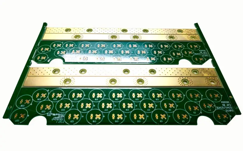
PCB boards are generally made of copper clad laminates. When selecting the boards, the electrical performance, reliability, processing requirements and economic indicators should be considered. Common copper clad laminates are copper clad phenolic paper laminates, copper clad epoxy paper laminates, copper clad epoxy glass cloth laminates, copper clad epoxy phenolic glass cloth laminates, copper clad polytetrafluoroethylene glass cloth laminates, and epoxy glass cloth for multilayer printed circuit boards. Laminates made of different materials have different characteristics. Epoxy resin and copper foil have excellent adhesion, so the adhesion strength and working temperature of copper foil are high, and it can not bubble in the molten tin at 260 ℃. The glass cloth laminate impregnated with epoxy resin is less affected by moisture. The UHF circuit board should preferably be coated with copper PTFE glass cloth laminate. For electronic equipment requiring flame retardant, flame retardant PCB boards are also required. These PCB boards are all laminates immersed in flame retardant resin.
PCB board size
The thickness of the PCB should be determined according to the function of the PCB, the weight of the installed components, the specification of the PCB socket, the overall dimensions of the PCB and the mechanical load it bears. It should mainly ensure sufficient rigidity and strength.
Common PCB board thicknesses are 0.5mm, 1.0mm, 1.5mm and 2.0mm.
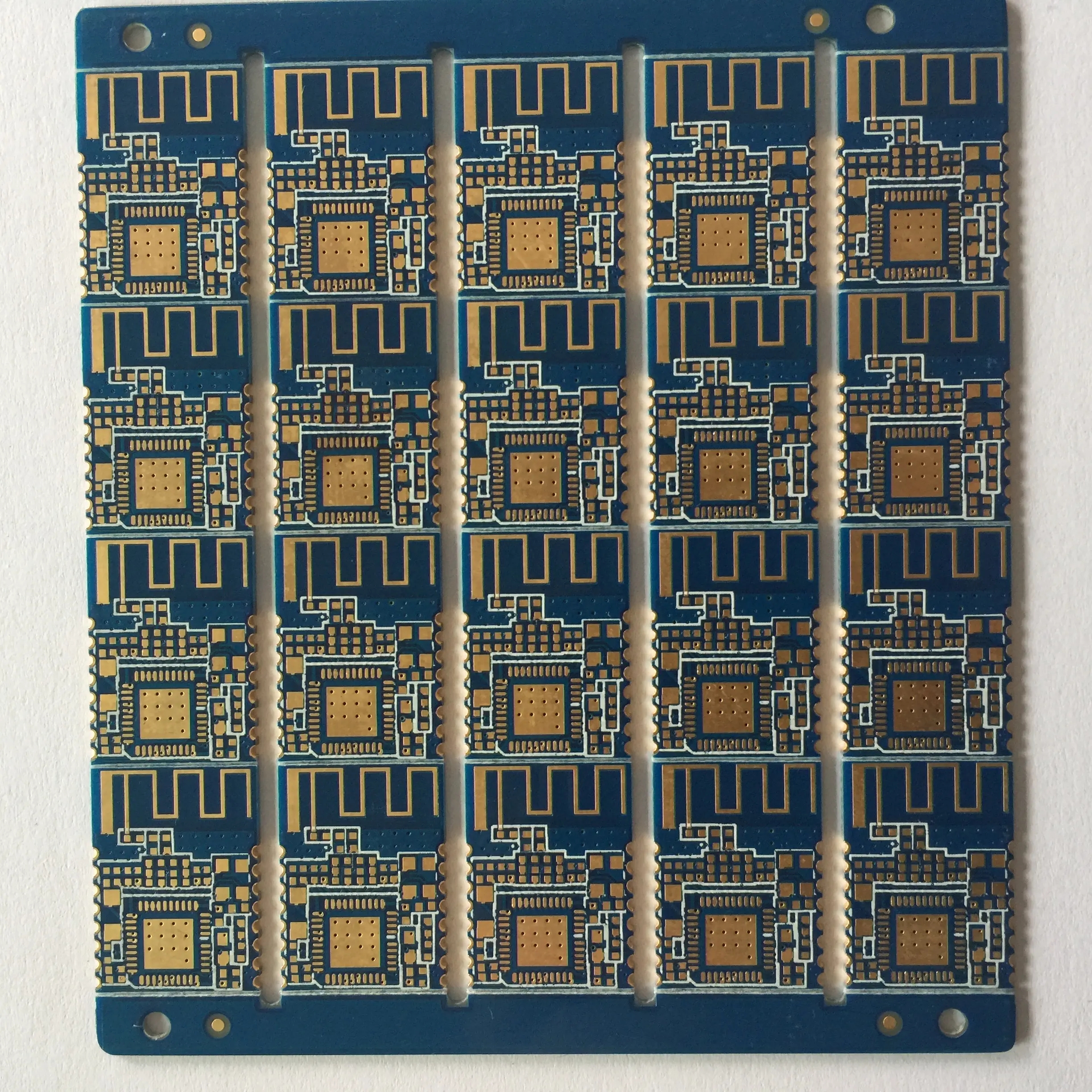
Considering the cost, copper film wire length and noise resistance, the smaller the PCB size, the better. However, if the size of PCB board is too small, the heat dissipation is poor, and adjacent wires are easy to cause interference. The cost of PCB production is related to the area of PCB. The larger the area, the higher the cost. When designing a PCB board with a chassis, the size of the PCB board is also limited by the size of the chassis. You must determine the size of the chassis before determining the size of the PCB board, otherwise you cannot determine the size of the PCB board. Generally, the wiring range specified in the prohibited wiring layer is the size of the PCB board.
The best shape of PCB is rectangle, and the length width ratio is 3:2 or 4:3. When the size of PCB is greater than 200 * 150mm, the mechanical strength of PCB should be considered. In a word, the advantages and disadvantages should be considered comprehensively to determine the PCB size.
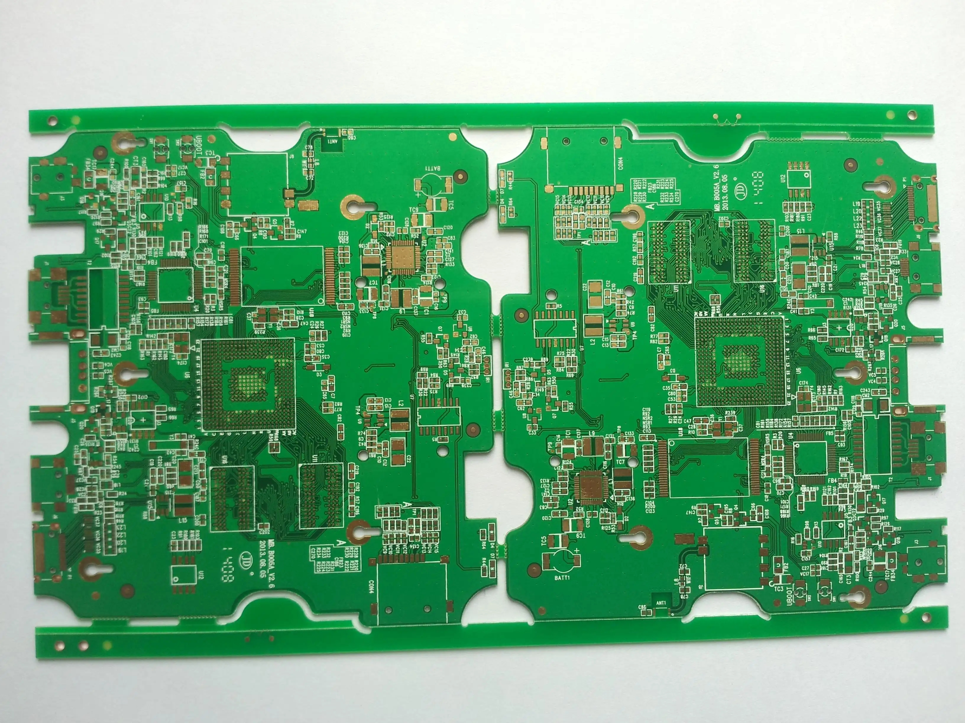
PCB board component layout
Although Protel DXP can automatically layout, in fact, component layout of PCB board is almost completed manually during design. PCB component layout generally follows the following rules:
1. Special component layout
The layout of special components shall be considered from the following aspects:
1) High frequency element
The shorter the connection between high-frequency components, the better. Try to reduce the distribution parameters of the connection and the mutual electromagnetic interference. The components that are vulnerable to interference cannot be too close. The distance between the components that belong to the input and those that belong to the output should be as large as possible.
2) Elements with high potential difference
The distance between the element with high potential difference and the connecting wire should be increased to avoid damaging the element in case of accidental short circuit. In order to avoid creepage, it is generally required that the distance between copper film wires of 2000V potential difference should be greater than 2mm. For higher potential difference, the distance should also be increased. Devices with high voltage should be arranged in places where it is not easy to reach during commissioning.
3) Components that are too heavy
Such components should be fixed by brackets, while large, heavy and heat generating components should not be installed on PCB boards.
4) Heating and thermal sensor
Note that the heating element should be far away from the thermal sensor.
5) Adjustable elements
For the layout of adjustable components such as potentiometers, adjustable inductance coils, variable capacitors, microswitches, etc., the structural requirements of the whole machine should be considered. If it is adjusted inside the machine, it should be placed on the PCB where it is easy to adjust. If it is adjusted outside the machine, its position should correspond to the position of the adjustment knob on the chassis panel.
6) Circuit board mounting hole and bracket hole
The mounting holes of the PCB board and the bracket should be reserved, because wiring is not allowed near these holes and holes.
2. Layout according to circuit function
If there is no special requirement, the components shall be arranged according to the element arrangement of the schematic diagram as far as possible. The signal shall enter from the left, output from the right, input from the top, and output from the bottom. Arrange the position of each functional circuit unit according to the circuit flow to make the signal flow more smooth and keep the direction consistent. With each functional circuit as the core, the layout shall be carried out around this core circuit. The element arrangement shall be uniform, neat and compact. The principle is to reduce and shorten the leads and connections between each element. The digital circuit part shall be arranged separately from the analog circuit part.
3. Distance from component to PCB edge
All components should be placed within 3mm from the edge of the PCB, or at least the distance from the edge of the PCB is equal to the thickness of the board. This is because the assembly line plug-in and wave soldering in mass production should be provided for the use of the guide rail slot, and it is also to prevent the PCB edge from being damaged due to the shape processing, which causes the copper film line to break and lead to waste products. If there are too many components on the PCB and they must exceed 3mm, 3mm auxiliary edges can be added on the edge of the PCB, and V-shaped grooves can be cut on the auxiliary edges, which can be broken by hand during production.
4. Sequence of component placement
First, place the components at fixed positions closely matched with the structure, such as power sockets, indicator lights, switches and connecting plug-ins. Then place special components, such as heating elements, transformers, integrated circuits, etc. Finally, place small components, such as resistors, capacitors, diodes, etc.
PCB manufacturers, PCB designers and PCBA manufacturers will explain the selection and size of PCB and the layout of PCB components.


Just upload Gerber files, BOM files and design files, and the KINGFORD team will provide a complete quotation within 24h.