
Professional PCB manufacturing and assembly
Building 6, Zone 3, Yuekang Road,Bao'an District, Shenzhen, China
+86-13410863085Mon.-Sat.08:00-20:00

Detailed explanation of writing skills of PCB design rule checker
With the rapid development of electronic technology, printed circuit boards are widely used in various fields, and almost all electronic devices contain corresponding printed circuit boards. In order to ensure the normal operation of electronic equipment, reduce mutual electromagnetic interference, and reduce the adverse impact of electromagnetic pollution on human beings and the ecological environment, electromagnetic compatibility design cannot be ignored. This paper introduces the design method and skills of printed circuit board.
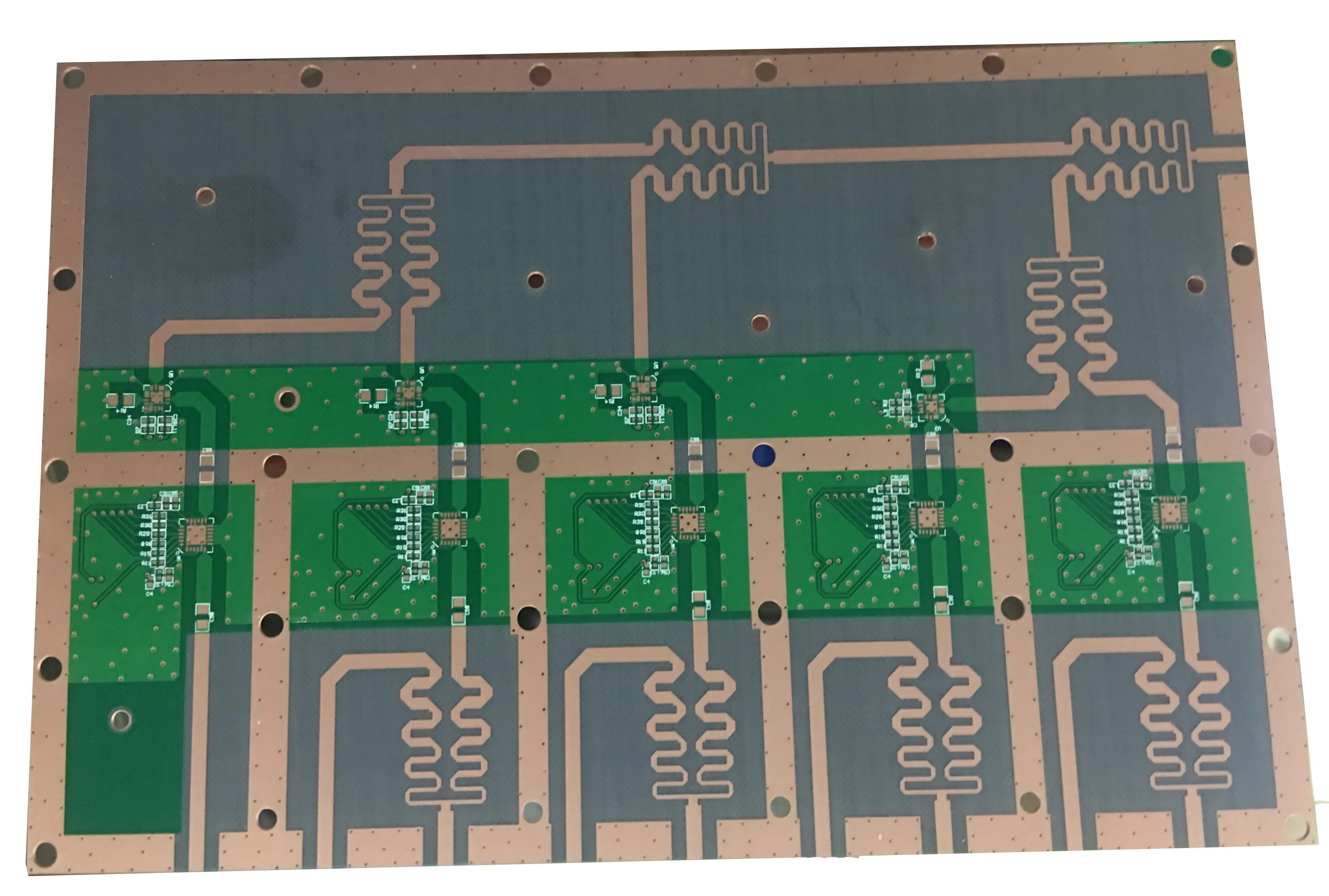
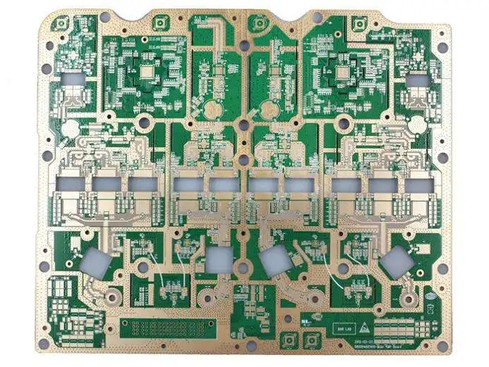
In the design of printed circuit board, the layout of components and the wiring of circuit connections are two key links.
layout
Layout refers to placing circuit components in the wiring area of printed circuit board. Whether the layout is reasonable not only affects the subsequent wiring work, but also has an important impact on the performance of the entire circuit board. After ensuring the circuit functions and performance indicators, to meet the requirements of processability, detection and maintenance, the components should be evenly, neatly and compactly laid on the PCB, and the leads and connections between components should be reduced and shortened as far as possible to obtain uniform assembly density.
Writing your own PCB design rule checker has many advantages. Although the PCB design checker is not so simple, it is not unattainable. Because any PCB designer who is familiar with existing programming or scripting languages can completely design a PCB design checker, the benefits of this work are incalculable.
However, general tools for marketing are usually not flexible enough to meet specific PCB design needs. Therefore, customers must reflect new feature requirements to DRC tool developers, which usually requires a certain amount of money and time, especially when the requirements are constantly updated. Fortunately, most tool developers can provide customers with convenient ways to write their own DRCs to meet specific needs. However, this powerful tool has not been widely recognized or used. This article provides a practical guide to maximizing the benefits of DRC tools.
Because DRC must traverse the entire PCB design circuit diagram, including each symbol, each pin, each network, and each attribute, it can also create unlimited "attached" files if necessary. DRC can mark any minor deviation that violates PCB design rules. For example, one of the attached files may contain all decoupling capacitors used in PCB design. If the capacitance is lower or higher than the expected value, a red mark will be marked where the dv/dt problem of the power line may occur. These attached files may be necessary, but not all commercial DRC tools can create these files.
Another advantage of DRC is that it is easy to update to meet the needs of new PCB design features (such as those that may affect PCB design rules). Moreover, once you have gained sufficient experience in this field, you can realize many other functions.
PCB manufacturers, PCB designers and PCBA manufacturers will explain the skills of PCB design rule checkers.


Just upload Gerber files, BOM files and design files, and the KINGFORD team will provide a complete quotation within 24h.