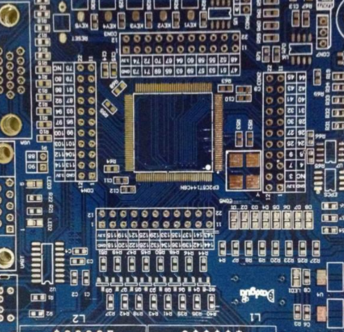
Common Problems in FPC Design
1 Overlapping FPC pad
1.1. Overlap of pads (except surface pads) refers to overlapping holes. Repeated drilling at one location may lead to breakage of the drill bit and damage during drilling.
1.2. Two holes in the multilayer board overlap, for example, one hole is the isolation plate, and the other hole is the connection plate (spline assembly plate). In this case, the negative pole was drawn out as the isolation plate, resulting in scrapping.
2. Abuse of graphic layers
2.1. Some useless connections are made on some graphic layers, but lines with more than five layers are designed instead of four layers, which leads to misunderstanding.
2.2. The design time chart is effortless. Take Protel software as an example, draw lines with layers for each layer, and mark lines with layers. In photo data, when no board layer is selected, due to the label line of the selected board layer, the circuit is lost and disconnected, or the circuit is short circuited, so the integrity and clarity of the graphic layer are maintained during the design.
2.3. It is inconvenient to violate the traditional design, such as the design of the bottom part surface and the design of the top welding surface.
3. Character confusion
3.1. Character cap SMD pad, which brings inconvenience to PCB damage detection and component welding.
3.2. The character design is too small, which makes screen printing difficult, and too large, which makes characters overlapping and difficult to distinguish.
4. Single side pad aperture setting
4.1. Single sided pads are usually not drilled. If holes need to be marked, the hole size shall be designed as zero. If a numerical value is designed, the coordinates of the hole will appear at this position, and problems will occur when generating drilling data.
4.2. Special labels shall be made for single-sided pads (such as drilled holes).
FPC

5. Drawing pads using filler blocks
Drawing boards with filler blocks can pass DRC check in circuit design, but are not suitable for processing. This type of pad cannot directly generate resistance data. When the upper resistor is used, the filler block area will be covered with solder, which makes the equipment assembly difficult.
6. The electric layer is patterned pad and connection
Since the power supply is designed as a pattern pad, this layer is opposite to the image on the actual PCB, and all connections are isolation lines, the designer should be very clear about this. By the way, care should be taken when drawing a complete set of power supplies or isolation lines in multiple places. No gap shall be left to short circuit two groups of power supplies or block the connection area (thus separating one group of power supplies).
7. Ambiguous definition of processing level
7.1. Single layer panel is designed at the top layer. If reverse and forward directions are not specified, the panel may be made of components and not well welded.
7.2. For example, a four layer circuit board is designed with four layers of top mid1 and bottom mid2, but it is not placed in this order during processing, which requires instructions.
8. Too many filler blocks or thin lines of filler blocks in the design
8.1. The photo data is lost and incomplete.
8.2. Since fill blocks are drawn one by one in photo data processing, the amount of photo data generated is quite large, which makes data processing more difficult.
9. The pad of surface mount device is too short
This is for on-off testing. For surface mounted equipment with excessive density, the distance between feet is very small and the base plate is very thin. To install the test pin, it must be at the staggered position of up and down (left and right). For example, the pad design is too short, which will not affect the equipment installation, but will not cause the test pin to be misaligned.
10. Large grid spacing is too small
The edges between the lines forming a large area grid are too small (less than 0.3mm). In the process of manufacturing printed circuit boards, it is easy to generate a large number of damaged films attached to the circuit boards after the development of the graphics conversion process, resulting in wire breakage.
11. Large area copper foil is too close to the outer frame
The large area of copper foil shall be at least 0.2mm away from the outer frame, because when milling the shape (such as copper foil), it is easy to cause the copper foil to warp and lead to the problem of flux falling off.
12. Ambiguous shape border design
Some customers have designed profiles, circuit board layers, top layers, etc. in the Keep layer These profiles do not coincide, which allows the FPC manufacturer to determine which profile line to use.
13. Uneven graphic design
The uneven coating caused by pattern electroplating affects the quality.
When the area of 14 layers of copper is too large, use grid lines to avoid foaming during SMT chip processing.
The above is the explanation given by the editor of pcb circuit board company.
If you want to know more about PCBA, you can go to our company's home page to learn about it.
In addition, our company also sells various circuit boards,
High frequency circuit board and SMT chip are waiting for your presence again.


