
Professional PCB manufacturing and assembly
Building 6, Zone 3, Yuekang Road,Bao'an District, Shenzhen, China
+86-13410863085Mon.-Sat.08:00-20:00


Solution to Electromagnetic Compatibility of PCB
Printed circuit boardis an important part of electronic equipment With the popularization of electronic technology and the development of integrated circuit technology, various electromagnetic interference problems emerge one after another, and the economic losses caused by electromagnetic interference are also increasing Therefore, electromagnetic compatibility becomes more and more important This paper aims to analyze the cause of electromagnetic interference (EMI) on PCB and discuss its avoidance methods
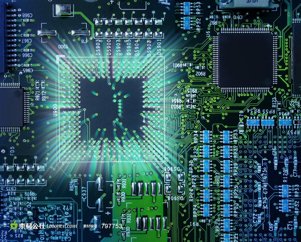
PCB board
EMI PCB

There are two main types of PCB interference One from PCB board This is mainly due to the parasitic coupling between adjacent circuits and the field coupling of internal components, resulting in the crosstalk of signals along the transmission path For example, capacitors turn on PCB s, especially those used in high-frequency applications We can regard it as LCR circuit, because when the capacitor actually works in the circuit, it usually generates equivalent inductance and impedance The capacitor has a self resonant frequency At the self resonant frequency, capacitors are capacitive Higher than self resonant frequency, capacitance is inductive, and impedance increases with increasing frequency Another kind of electromagnetic interference comes from PCB, which is divided into two types: radiated interference and sensitive components The radiation mainly comes from the harmonic source of clock and other periodic signals Some electronic equipment or instruments produce second harmonic due to voltage and power jump
Avoid PCB electromagnetic interference, mainly from the following points:
1. Reasonable design schematic diagram
When designing a circuit board, the first thing to do is to design the schematic diagram The design sketch is usually operated by Altium Designer software You can filter all used components in the schematic library If there is no component to select in the schematic library, you can draw it yourself After drawing the schematic diagram, automatic detection is required to check whether there are obvious errors in the drawing process After the sketch drawing is completed, the printed circuit board can be designed The result of automatic routing is always unsatisfactory and requires manual layout and routing When designing printed circuit boards, electromagnetic compatibility has become an important scientific and technological requirement to be considered The reasonable layout of components and circuits in PCB can effectively reduce EMI problems
2. Choose a capacitor whose equivalent inductance and resistance are relatively small
The problem of crosstalk should also be pay attention to According to Faraday electromagnetic induction phenomenon, when the wire passes through the current, a magnetic field will be generated around the wire The magnetic field interaction of different wires produces crosstalk Mutual inductance is one of the mechanisms of crosstalk, and its amplitude is proportional to the current in the conductor
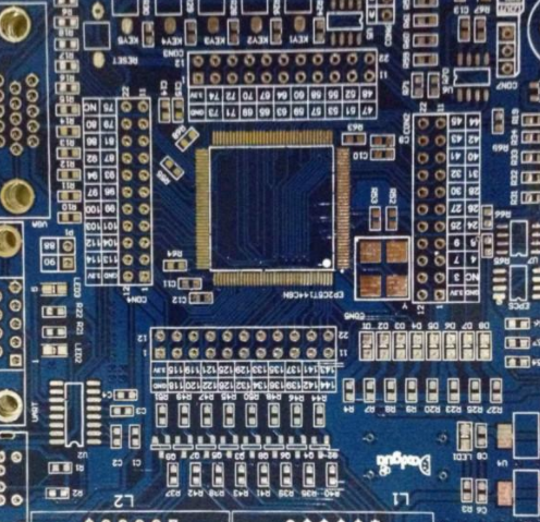
PCB board
3. Limit the periodic signal to an area as small as possible
Mutual capacity is another mechanism that products cross walk, which is produced by electric field coupling of two electrodes The solution is to limit the periodic signal to the smallest possible area and block the parasitic coupling path with the outside world If necessary, the screening program can be used for filtering; External sensitivity mainly includes radio frequency interference and electrostatic discharge, etc, To solve this problem, you can use masks, good grounding and filtering methods
4. Anti-interference methods when designing printed circuit boards
(1) Selection of PCB data Printed circuit boards are divided into single-sided, double-sided and multilayer boards Epoxy glass cloth is usually used as the base material This material has the following advantages: good expansibility, which is conducive to reducing loop area, reducing differential mode interference, low water absorption, heat resistance, chemical corrosion resistance, and impact resistance good
(2) the wiring of The PCB Follow the flux principle when wiring The principle of magnetic flux means that the magnetic lines of force generated by the transmission line and the return path cancel each other to realize the cancellation of magnetic flux A single panel has no ground plane, and the focus of its wiring is to reduce the loop area of power loop and signal loop Use protective grounding when wiring Unplug the ground wires close to the power line or signal line and wire them together to reduce the loop area High speed signal route shall be straight line or obtuse angle without acute angle or right angle
(3) The layout of the PCB Under normal circumstances, PCB design software has automatic layout function, but this function cannot meet the needs of actual work. In addition, designers need to be familiar with layout rules In the layout, the digital circuit part and the analog circuit part should be separated, leaving some space in the middle The layout should be based on high speed, medium speed and low speed, and I/O circuit zoning to reduce the interference of high speed circuit to other components
Conclusion
The design of the printed circuit board is a complicated process. Many factors need to be considered in the design process A little neglect will have a great impact on the effectiveness of the circuit board If electromagnetic compatibility is not fully considered in the design process, the designed circuit board may not be put into use normally Therefore, mask and other issues shall be fully considered in the design of wiring, layout and grounding to prevent cross talk between PCB signals


Just upload Gerber files, BOM files and design files, and the KINGFORD team will provide a complete quotation within 24h.