
Professional PCB manufacturing and assembly
Building 6, Zone 3, Yuekang Road,Bao'an District, Shenzhen, China
+86-13410863085Mon.-Sat.08:00-20:00

Detailed explanation of important assembly design rules of circuit board factory
The PCB design is completed because the PCB shape is too small to meet the production process requirements, or a product is composed of several PCBs, so it is necessary to assemble several small boards into a large board with an area meeting the production requirements, or to assemble multiple PCBs for a product to facilitate the production of electrical equipment. The former is similar to the stamp board. It can not only meet the PCB production process conditions, but also facilitate the electrical installation of components. It is very convenient to separate them when using; The latter is to assemble several sets of PCB boards of a product together, which is convenient for production and is also convenient for a complete set of products.
No matter what kind of PCB, it is usually necessary to use the panel structure. However, there are many ways of panel design, and sometimes it is difficult to determine which way to use and the number of panels, which requires comprehensive consideration of various factors.
There are generally two methods for PCB assembly, ABAB or AAAA. It is not easy to say which type of panel is good. This needs to be determined by considering the density and distribution of components on the panel and the equipment configuration. Both types of panel have their advantages and disadvantages.
1. ABAB, commonly known as mandarin duck board, yin and yang board, or front and back panel design, is characterized by symmetrical component distribution on both sides of the panel. The advantages of this design are that the equipment configuration is simple and easy, and the preparation operation before production is simple and easy. All SMT assembly needs only one preparation: a steel mesh, a set of patch procedure, SPI inspection procedure, reflow welding temperature curve, etc. However, for products with large difference in component distribution density on both sides of PCB, this may lead to other problems. In some product designs, most of the components may be concentrated on one side of the PCB, while there are only a few simple packaged components on the other side. This ABAB assembly method is not good. This design sometimes leads to printing and mounting problems of some fine pitch components. If there are high quality components on the board, sometimes it will also bring the risk of components falling down during the secondary reflux. Finally, for mass production, the equipment utilization rate will not be too high as a result of such splicing.
2. AAAA/BBBB, a non negative plate design, has the advantage of reasonably arranging equipment configuration and production process according to the distribution characteristics of components on the plate: size and density, and improving equipment utilization. Also, because the components with the same structure are on the same side of the panel, the production process can be reasonably arranged, for example, to avoid the printing short circuit of closely spaced components or the dropping of high profile and large quality components during the secondary reflow. The main disadvantage of this type of panel assembly is that the production and assembly of the two sides of the panel are completely different. Contrary to ABAB, all preparations, such as steel mesh, SPI inspection procedure, mounting procedure, AOI inspection, reflux temperature curve, etc., are different on both sides, and even the production line needs to prepare two, which is not applicable to small batch and multi model products. Of course, for large batches, if the production line configuration is tight, it is not recommended to be the preferred design. Especially in the NPI stage, it brings troubles to the production planning.
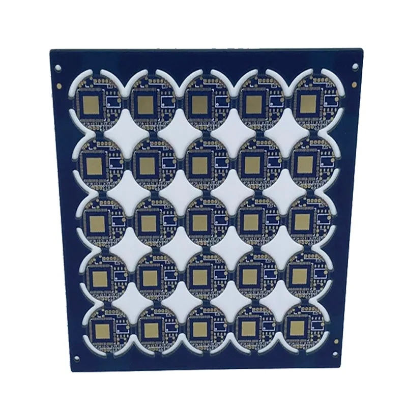
3. Sometimes multiple types of boards are spliced in one panel, which is also possible, as shown in the following figure. If the product contains multiple PCBs and the distribution of signal layers inside these boards is similar, this design can be considered.
Circuit board manufacturers, circuit board designers and PCBA manufacturers explain the important assembly design rules of circuit board manufacturers.


Just upload Gerber files, BOM files and design files, and the KINGFORD team will provide a complete quotation within 24h.