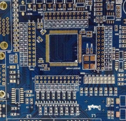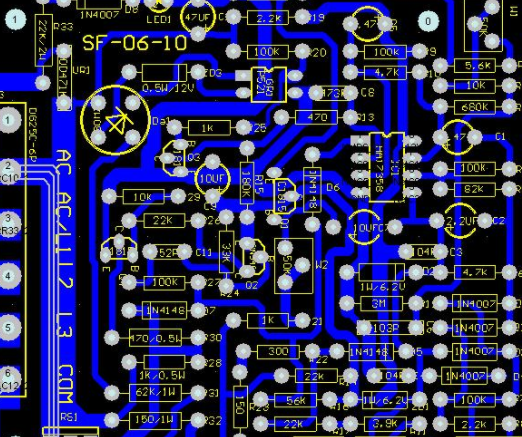
High frequency PCB board wiring rules
1 Component arrangement rules
1) Under normal conditions, all components shall be arranged on the printed circuit boardOnly when the top components are too dense, some equipment with limited height and low heat generation, such as chip resistors and chip capacitors, can be placed, Paste IC, etc On the ground floor
2.) On the premise of ensuring the electrical performance, components should be placed on the grid and arranged in parallel or vertical to make them neat and beautiful Generally, overlapping of parts is not allowed; The layout of components shall be compact and the input and output components shall be as far away as possible
3.) There may be a high potential difference between certain components or wires
4.) Components with high voltage should be arranged in places that are not easily accessible by hand during debugging
5.) Components located at the edge of the board, at least 2 board thicknesses away from the edge of the board
6) The components should be evenly distributed and uniform in density on the entire board surface.
PCB board

2. The principle of layout according to the direction of the signal
1) Usually, the position of each functional circuit unit is arranged one by one according to the signal flow, centered on the components of each functional circuit, and arranged around it
2) The layout of the components should facilitate the flow of signals and keep the signals in the same direction as possible. In most cases, the signal flow is arranged from left to right or from top to bottom, and the components directly connected to the input and output terminals should be close to the input and output connectors or connectors
3. Prevent electromagnetic interference
1) For components with strong radial electromagnetic fields and components sensitive to electromagnetic induction, the distance between them should be increased or masked, and the component placement direction should cross the adjacent printing lines
2) Try to avoid high and low voltage devices being mixed with each other
3) For components that generate magnetic fields, such as transformers, loudspeakers, inductors, etc, In the process of layout, attention shall be paid to reducing the magnetic line cutting of the printed circuit, and the magnetic field directions of adjacent components shall be perpendicular to each other to reduce the coupling between them
4) Shield the interference source
5) For circuits operating at high frequencies, the influence of distribution parameters between components should be considered
4. Suppress thermal interference
1) For the heating element, it shall be arranged at a position favorable for heat dissipation If necessary, the radiator or small fan can be set separately to reduce the temperature and the influence on adjacent components
2) Some integrated blocks, large and medium-sized power tubes, resistors and other high power consumption components shall be arranged at places where heat dissipation is easy and shall be separated from other components
3) The thermal element should be closed to the measured element and away from the high temperature area, so as to avoid faults caused by other heating power equivalent elements
4) When placing components on both sides, heating components are usually not placed on the bottom layer
5. The layout of adjustable components
For the layout of adjustable components such as potentiometers, variable capacitors, adjustable inductance coils or microswitches, the structural requirements of the whole machine shall be considered If the adjustment is made in the machine, it should be placed in the position of the adjustment printed circuit board
Design PCB
Surface mount circuit board is one of the indispensable components in surface mount design SMT circuit board is the support of circuit components and devices in electronic products. It realizes the electrical connection between circuit components and equipment With the development of electronic technology, the size of PCB is smaller and smaller, the density is higher and higher, and the number of PCB layers is increasing Therefore, the PCB requires anti-interference capability, technology and manufacturability in the overall layout The requirements are getting higher and higher
The main steps of printed circuit board
1) Draw a schematic diagram.
2) Creation of component library.
3) Establish the network connection relationship between the schematic diagram and the components on the printed board.
4) Wiring and layout.
5) Create printed board production usage data and placement production usage data.
The following issues shall be considered in the design process:
1) It is necessary to ensure that the component graphics of the circuit schematic diagram are consistent with the real object and that the network connection in the circuit schematic diagram is correct.
2) The design of the printed circuit board not only considers the network connection relationship of the schematic diagram, but also considers some requirements of circuit engineering The requirements of circuit engineering mainly include the width of power line, ground wire and other wires, connection of lines, high-frequency characteristics of some components, component impedance, anti-interference, etc
3) The installation requirements of the whole system of the printed circuit board mainly consistent that the installation holes, plugs, locating holes, reference points, etc The requirements must be met. The placement of each component must be accurately installed in the specified position. At the same time, it is necessary to facilitate installation, system commissioning, ventilation and heat dissipation
4) The manufacturability of the printed circuit board and its technical requirements must be familiar with the design specifications and meet the production process requirements, so that the designed printed circuit board can be successfully produced
5) Considering that the components are easy to install, debug The PCB must be standardized to ensure that there is no collision between components for easy installation
6) The purpose of designing a printed circuit board is mainly for application It is beneficial to improve reliability, reduce the number of vias, optimize wiring, make its density and consistency uniform, and make the overall layout of the circuit board more beautiful To make the designed circuit board achieve the desired purpose, the overall layout of the printed circuit board and the placement of components play a key role, which directly affects the installation, reliability, ventilation and heat dissipation of the entire printed circuit board, as well as the direct wiring Speed
The external dimensions of the printed circuit board are preferred When the PCB board is too large, the printed lines will be very long, the impedance will be increased, the noise resistance will be reduced, and the cost will also be increased If it is too small, the heat dissipation is poor, and adjacent lines are vulnerable to interference, First, provide reasonable positioning PCB for size and shape Then determine the location of special components and unit circuits, etc, According to the circuit flow, the whole circuit is divided into several unit circuits or modules, and the center the components of each unit circuit (such as integrated circuits) and other components must be in a uniform order, arranged neatly and compactly on the PCB, but not too close to these large components, and there must be a certain distance, especially some relatively large and relatively high components, This facilitates welding and rework For high power integrated circuits, color heat sink shall be considered, enough space shall be reserved for it, and it shall be placed in a well ventilated place of printed circuit board At the same time, don't focus too much There must be a certain distance between several large components on the same plate. Their direction should be 45 degrees Smaller integrated circuits such as (SOP) should be arranged in the axial direction. The components are vertically and axially aligned, all of which are related to the transportation direction of the PCB board in the production process With this kind of pipe, the components are arranged in order to reduce welding defects LED for display, etc, It should be considered to place on the edge of the printed board, as they are used for observation during application Some switches, trim elements, etc It should be placed in an accessible place In the same frequency circuit, the distribution parameters between components shall be considered In general, distribution parameters between components should be considered in high frequency circuits In general, the components should be arranged as parallel as possible, which is not only beautiful, but also easy to install and weld Easy for mass production, components located at the edge of the circuit board must be 3-5 cm away from the edge When considering the position of components, the thermal expansion coefficient, thermal conductivity, data heat resistance and bending strength of PCB shall be fully considered to avoid the impact on components or PCB during production After determining the position and shape of components on PCB, the PCB wiring is considered


