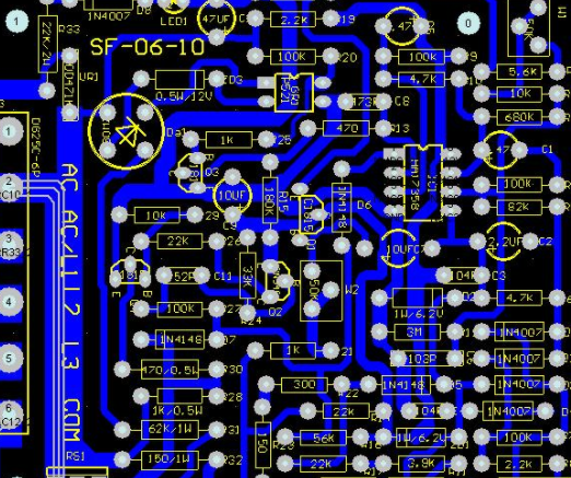
Several Problems Should Be Considered in PCB Design
With the vigorous development of the PCB industry, more and more engineers and technicians have joined in designing and manufacturing PCB boards However, because many PCB manufacturing industries and a considerable number of PCB design engineers (Layout staff) I have not added in or separated in the production and manufacturing process of PCB boards are involved, power efficiency and product functions are emphasized in the design process, but downstream PCB processing plants receive orders In the actual production process, due to the lack of consideration of the difficulties of product processing, there are many problems in the design, the extended processing cycle or the hidden danger of the product, which are unfavorable to the processing and production. To facilitate the expression, from the seven aspects of cutting, drilling, wiring, welding mask, role, surface treatment and forming analyze:
PCB board

1. Opening mainly considers the plate thickness and copper thickness:
For plates with a thickness greater than 0.8MM, the standard series is: 1.0, 1.2, 1.6, 2.0, 3.2 mm. Plate thickness less than 0.8MM is not considered as the standard series 0.40.6 mm, this data is mainly used for the inner layer of multilayer plates When selecting the thickness of the outer layer, pay attention to the thickness of copper plating, welding mask, surface treatment (tin scattering, gold plating, etc.) and thickness of characters and carbon oil, The tin plate thickness will be greater than 0.075-0.15 mm For example, when the finished product requires a thickness of 2 0 mm, when 2. usually select 0 mm plate for cutting, considering the plate tolerance and processing tolerance, the thickness of finished plate will reach 2.1-2.3 mm If the design requires that the thickness of the finished product should not be greater than 2.0 mm, the circuit board should be made of a 9 mm non-traditional plate The PCB processing factory needs to temporarily order from the circuit board manufacturer, and the lead time will become very long When making the inner layer, the thickness after placement can be adjusted by the thickness and structural configuration of the pressing (PP), and the selection range of core boards can be flexible MM can also be 1.0mm, as long as the thickness of the laminate is controlled within a certain range to meet the thickness requirements of the finished product In addition, there is the problem of plate thickness tolerance When considering the product assembly tolerance, PCB designers should also consider the thickness tolerance PCB processing There are three main aspects that affect the tolerance of finished products: plate tolerance, lamination tolerance and outer layer thickening Tolerance Seven conventional sheet tolerances are now provided for reference: (0.8-1.0) ± 0.1 (1.2-1.6) ± 0.13 2.0 ± 0.18 3.0 ± 0.23 Laying tolerances are controlled within ± (0.05-0.1) according to different layers and thicknesses between MM. Specially for boards with board edge connectors (such as printed plugs) The thickness of the surface copper is a problem because the hole copper needs to be chemically dipped and plated. If no special treatment is carried out, when the hole copper is thickened, the thickness of the surface copper will be thickened together According to IPC-A-600G standard, the copper plating thickness of Class 1 and Class 2 is 20um, and that of Class 3 is 25 microns Therefore, when making a circuit board, if the copper thickness requires 1OZ (30.9 μ m), sometimes it will be based on the wire cutting data Select HOZ (15.4 μ m) for width/line spacing, except for the allowable tolerance of 2-3 μ m, can reach 33.4um If you select 1OZ for cutting, the thickness of finished copper will reach 47.9um Other copper thickness calculations can be derived, etc
2. The non metalized hole and the design of the positioning hole:
At present, the machining tip of mechanical drilling is 0.2mm. However, due to the thickness of copper on the hole wall and the thickness of the protective layer, the design aperture needs to be increased in the production process, the tin spraying plate needs to be increased by 0.15mm, and the gold plate needs to be increased by 0.1mm The key question here is, if the hole diameter is increased, does the distance from the hole to the circuit and the copper sheet meet the processing requirements? Is the land of the originally designed circuit pad sufficient? For example, the through-hole diameter is 0.2 mm and the gasket diameter is 0.35 mm Theoretical calculation shows that 0. 075mm on one side of the welding ring can be fully processed, but the drill nozzle after production is expanded according to the tinplate, without welding call. If due to the spacing problem, the CAM engineer cannot make the gasket larger and cannot make the circuit board Aperture tolerance: At present, the drilling tolerance of most domestic drilling rigs is ± 0.05 mm. With the tolerance of coating thickness in the hole, the tolerance of metallized hole is controlled at ± 0.075 mm, and the tolerance of nonmetallic hole is controlled at ± 0.05 mm Another problem that can easily be ignored is the isolation distance from the drilled hole to the inner layer of copper or conductor of the multilayer plate Since the drilling positioning tolerance is ± 0.075mm, there is a ± 0. 1mm tolerance change of the inner laminate graphics expansion and deformation during lamination Therefore, in the design, the distance between the hole edge and the conductor or copper sheet shall be ensured to be greater than 0.4 layers of 15 mm, and the isolation of 6 or 8 layers of plates shall be ensured to be greater than 0.2 mm, which is convenient for production There are three common methods for making nonmetallic holes: dry film sealing or gel plugging. Since there is no corrosion protection, the copper plating in the holes can be removed during the etching process Pay attention to the dry film seal. The hole diameter shall not be greater than 6.0mm, and the plug hole of rubber particles shall not be less than 11.5mm In addition, secondary drilling is used to make non-metallic holes No matter what method is used, there shall be no copper sheet within the range of 0. 2mm around the nonmetallic hole The design of locating hole is often a problem easy to ignore In the process of circuit board processing, test, shape punching or electric milling, holes larger than 1. It is necessary to use 5mm as the positioning hole for board fixing In design, it is necessary to consider forming 3 corners as much as possible and distributing holes on 3 corners of the circuit board
3. Circuit fabrication mainly considers the influence of circuit etching
Due to the influence of lateral corrosion, in the production and processing process, the thickness of copper and different processing technologies are considered, and the circuit needs to be pre thickened The traditional tin spraying gold plating HOZ copper compensation is 0.025mm, the traditional compensation of 1OZ copper thickness is 0.05-0.075mm, and the line width is 0.05-0.075mm/ The production line spacing and processing capacity are usually 0.075/0.075 mm Therefore, it is necessary to consider compensation during production when considering line width/line spacing wiring Since the gold coating on the circuit does not need to be removed after the gold plate is etched, and the line width has not been reduced, no compensation is required However, it should be noted that since the side etching still exists, the line width of the copper skin under the gold layer will be smaller than that of the gold layer If the copper is too thick or etched excessively, the gold surface is easy to collapse, resulting in poor welding For lines with characteristic impedance requirements, line width/line spacing requirements will be more stringent
4. The more troublesome solder mask production is the solder mask treatment method on the vias:
In addition to the conductive function of the via, many PCB design engineers will design it as a finished online test point after assembly of components, and even some will be designed as component holes Traditional through-hole design is used to cover oil to prevent tin plating during welding If it is used as a test point or insertion hole, the window must be opened However, it is easy to cause the tin bead to be hidden in the hole by spraying the tin plate with cover oil Therefore, a considerable number of products are designed to be plugged with oil In order to facilitate the packaging at the BGA location, it is also treated according to the blocked oil However, when the aperture is greater than 0 6 mm, it will increase the complexity of plugging the oil (the plug is not full) Therefore, the tin spraying plate is also designed as a half open window, with a single side 0. 065mm larger than the hole diameter, and the hole wall and hole edge within 0. 065mm Tin spraying
5. Character processing mainly considers adding pads and related marks on characters
With the increasingly dense component layout, it is necessary to consider that the pad cannot be placed on the character printing, at least to ensure that the distance between the character and the pad is greater than 0.15 mm, and sometimes the component frame and component symbols cannot be completely distributed on the circuit board Most films are made by machines. In summary, if it is really impossible to make adjustments during the design process, you can consider printing character frames only, not component symbols The content usually added to the logo includes supplier logo, UL demonstration logo, flame retardant grade, anti-static logo, production cycle, customer designated logo, etc It is necessary to clarify the meaning of each marking and to set aside and specify additional positions
The above is the explanation given by the editor of pcb circuit board company.
If you want to know more about PCBA, you can go to our company's home page to learn about it.
In addition, our company also sells various circuit boards,
High frequency circuit board and SMT chip are waiting for your presence again.


