
Professional PCB manufacturing and assembly
Building 6, Zone 3, Yuekang Road,Bao'an District, Shenzhen, China
+86-13410863085Mon.-Sat.08:00-20:00


The Design of Digital Display Thermometer PCB
1 Introduction
With the development of science and technology and the rapid progress of industrial technology, we often need to accurately measure and control the ambient temperature and equipment temperature in daily production Therefore, it is very important to study the measurement and control of temperature We want to feel the temperature from the outside. The key is the temperature sensor, which is completed with LM3.5 After obtaining the temperature value of the external world, a specific display device is required to display it The current popular method is to use a/D converter, which is completed with ICL7107 Then display through LED or LCD The thermometer described below is displayed by dual common anode digital tube (LED).
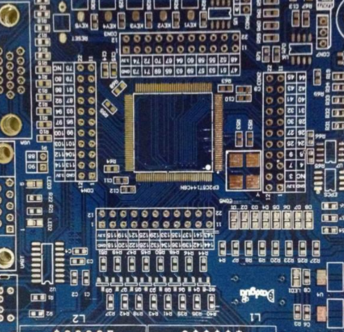
PCB board

2. The problems that need attention
If we want to successfully design the schematic diagram of the PCB thermometer, we usually go through the following steps: First, learn to draw the schematic diagram of the thermometer We must build a component library (Sch. Library) to meet the design needs You can select components from the components in Browse Schlib, and then describe it in the Description (Description, Footprint, Default Manifesto, Sheet part Filename) We must pay attention to some minor problems when making components. For example, when making TL431 component symbols, the pins are not placed on the grid. When converting to the schematic diagram, the wires cannot be connected properly, and no nodes can exist on the pins At this point, we can right-click in the production window to select the document option, and set the "Snap" and "Visible in the Grid" options in the pop-up "Library Editor Workspace" dialog box When making components, you should also pay attention to skills For example, with the help of similar components in the existing component library, copy them to your own product library and make minor modifications When manufacturing the integrated chip Icl7107, Icl7660, S-DSP, you must pay attention to the content of each pin. You must carefully set them one by one to avoid incorrect connection in the schematic diagram, which will cause the chip to burn out during debugging The second small step is to transfer the components to be used to the schematic diagram for connection During connection, pay attention to the connection of bus bars Busbar is only a schematic power connection, and the real connection is a network label Therefore, the network label must be placed when using the bus bar Step 3: After connecting the circuit diagram, we must execute ERC, report/bill of materials, and create a netlist Check the power rules to correct circuit errors in the circuit diagrams Run a component report to view component information for a circuit diagram Create a net list to prepare for PCB drawing The schematic diagram of the design mainly consists of the following parts The second step is to complete PCB production Making PCB board, determining the physical size, wiring size and various required board layers of the circuit board frame can be completed through the wizard Step 2: In defining PCB, call menu column command Design/Load Network to transfer components to PCB When placing components, it should be noted that different components need to be placed on different layers, such as placing names (Pinyin) in the BottomLayer layer, and horizontal images. Chinese characters cannot be used Step 3 is to select the via type of jumper Step 4: Select the number of copper film lines passing between the component type and the pad, and call the menu command Design/Rules to be set The fourth step is to set the routing parameters Step 5: After connecting the PCB board, you need to check the design rules and call the menu command tool/design rule check This can be done to avoid design errors and power errors
3. Printing, copper foil transfer, corrosion treatment and problem PCB diagram
1) Print the PCB diagram to the thermal transfer paper with a laser printer (use the thermal transfer paper to make the PCB)
Add a printer in the start menu, and follow the steps of the add printer wizard (if there is no actual printer connected, you can choose a printer, Select the layer to be printed and set: set the bottom layer of the printed graphic as the upper layer in the "Layer" column, select "Show Holes" in the "Options" column, nSelect Black&White (black and white graphics) in the Color Set column In the design PCB diagram, place a "string" on the bottom layer, and write your name (Chinese Pin in) and design date in it The name and date shall be horizontally mirrored Once set, print the bottom graphic onto the heat transfer paper
2) Cutting material: cut the copper clad plate according to the size, polish it with fine sandpaper
3) transfer the bottom layer of the printed PCB to the copper card board with a thermal Transfer machine
4) Repair the board: repair a small amount of unprinted lines with quick-drying paint
5) Corrosion: Put the copper-clad board with the printed circuit board into the ferric chloride solution to corrode. If the solution concentration is high and the temperature is high, the corrosion rate is fast, but the concentration and temperature should be appropriate Master the corrosion time
6) Wash and dry
7) Drilling holes, select a drill with a proper diameter: drill with a diameter of 0, integrated circuit pin, universal resistor and capacitor 8mm If the component pin is thicker, you can replace the drill bit with a larger diameter according to the measured value During drilling, the drill bit shall be inserted into the clamp as deep as possible, and the clamp shall be tightened
8) Remove the ink on the wrapper film: Use organic solvent (alcohol, banana water, acetone, etc.) to wipe off the ink covering the wrapper film line When the above solvents are not available, they can also be wiped off with sandpaper
9) Sand and check the circuit board: After removing the ink, polish the copper film conductor with finer sandpaper The better ground, the better welded However, do not over polish to avoid excessive loss of copper film thickness After polishing, clean with paper towel Check the circuit board: use a multimeter to check whether there is short circuit or open circuit between the lines on the circuit board PCB If there is a short circuit, it should be cut off. If there is an open circuit, it should be welded and connected
10) Flux: Dissolve rosin in anhydrous alcohol to make flux for use. Note that the concentration of flux should be appropriate Too thick, not bright after drying, too thin, poor welding efficiency Use a brush to evenly smear the alcohol rosin flux on the clean surface of PCB board When brushing the teeth, place the PCB board in the vertical direction to avoid the flux blocking the drilling Just brush it once Brushing too many times is easy to wrinkle and will not give off light Place the PCB board coated with alcohol rosin flux and dry it in the sun or naturally ICL7107 is a decimal double integral 3-bit analog-to-digital converter with an accuracy of ±2LSB (effective bit). When its typical reference voltage is 100 They are 0 mV and 1000 mV respectively, and the corresponding peripheral integrated resistance and integrated capacitor are selected. They can be two types of circuits, with full scale of 200 mV and 2000 mV. The analog circuit consists of switches and operational amplifiers to achieve signal sampling and integration Differential input is adopted, and the input impedance is 1O10 Ω) Digital circuit consists of counter, latch, control logic and display decoder The input analog signal voltage value is first converted into a time width signal proportional to it, and then a fixed frequency clock pulse is calculated within this time width. The counting result is proportional to the number of input analog signals, and digital locking is performed Save and decode the display


Just upload Gerber files, BOM files and design files, and the KINGFORD team will provide a complete quotation within 24h.