
Professional PCB manufacturing and assembly
Building 6, Zone 3, Yuekang Road,Bao'an District, Shenzhen, China
+86-13410863085Mon.-Sat.08:00-20:00

PCB Design of NiMH Battery Charger Circuit
1. Protel Software Introduction
With the rapid development of electronic information technology, manually designed PCB (printed circuit board) of electronic products can no longer meet the needs of the development of electronic technology. We must use computers to complete PCB design, which is not only fast and accurate, but also can greatly reduce the labor intensity of engineering and technical personnel. There are many kinds of software involved, and Protel is a classic one.
Protel is a circuit aided design system launched by Altium. It is the first board level design system that integrates all design tools, including schematic design, PCB design, circuit simulation, PLD design, etc. Its earliest version was the TANGO software package, which later developed into Protel for DOS, Protel for Windows, Protel 98, Protel 99 SE, Protel DXP and Protel 2004. With the continuous upgrading of the version, its functions become more and more powerful.

Compared with other versions, Protel 2004 has many new functions, which make the operation simpler and more automatic, and enable us to easily design various complex circuit boards.
2. PCB design
PCB is the abbreviation of Printed Circuit Board in English, which is translated as printed circuit board, or PCB for short. Printed circuit board is made of conductive circuit and component package by printing. Its main function is to realize the fixed installation of electronic components and the electrical connection between pins, so as to realize various specific functions of electrical appliances. Making correct, reliable and beautiful printed circuit board is the ultimate goal of circuit board design.
The general process of PCB design includes: preparation for production, production of PCB component pin package, creation of PCB file, planning of circuit board, loading of component pin package and network, layout, wiring, DRC design rule check, etc.
3. PCB Design of Ni MH Battery Charger
Ni MH battery charger is a common electronic product in our life. The basic steps for designing the printed circuit board (PCB) of this circuit with Protel 2004 are as follows.
3.1 Creating Project Files
To facilitate the management of design documents, seamless connection and synchronous design between them. Project files are used for management in Protel 2004. First, create a project file, and then create or add each design file under the project file.
3.2 Create schematic file and complete schematic design of battery charger circuit
3.3 Create PCB file and plan
There are two ways to create PCB files in Protel 2004: using the file menu to create PCB files and using the wizard to create PCB files. Note that the PCB files created with the wizard are not in the project file. After the creation, they must be put into the project file, otherwise the following steps will not be possible. According to the composition of the charger circuit, the shape of the board is first planned to be rectangular, and the size of the board is determined to be 2400mil according to the number of components × 1300mil, single-layer cabling is designed as a single panel.
3.4 Load component pin package and network and perform component layout
All components in this circuit are in the form of jack package. In addition to the positive polarity packaging of the battery pack, other components are packaged using the standard packaging in the Protel 2004 component library. We need to set the packaging for the positive polarity end of the battery pack according to the actual circuit. First, create your own component packaging library, create the packaging shown in BT1-BT4 in the library, and then set this packaging as the packaging of the battery pack.
The component layout can be carried out automatically and then manually. Note that the transformer is not placed on this board. During the layout, the arrangement and distribution of components shall be reasonable and even, and shall be as neat and beautiful as possible, meeting the requirements of circuit structure and process.
3.5 Setting Wiring Rules and Wiring
The so-called "wiring" refers to the use of printed wires to complete the wiring relationship of components in the schematic diagram. After the component layout of any circuit board is completed, the next thing to do is to connect the components with wires to make them have electrical characteristics, so as to form a complete circuit board.
In Protel 2004, the wiring rules must be set first to meet the electrical requirements such as safety principles. According to the actual requirements of the charger circuit, the safety distance is set as 10mil, the top layer wiring, the common line width is 10mil, the power line is 20mil, and the ground wire is 30mil Automatic wiring is adopted for wiring, and the unqualified places can be manually modified finally. On the premise of meeting the electrical requirements such as the safety principle, the wires should be simplified, as short as possible, with as few turns as possible, and the wires should be simple and clear.
In addition, the wiring design shall consider whether the assembly is convenient. Finally, the board is required to be beautiful and economical. A good PCB board has beautiful wiring and fine work, which looks like a work of art.
3.6 DRC design rule check and error elimination.
After the circuit board design is completed, in order to ensure that the design work carried out meets the requirements, the computer can automatically complete the inspection work, that is, DRC design rule inspection. After the inspection, the system will pop up the Messages message box, and modify the design according to this message until there is no error. At this point, the PCB design of the circuit is completed. The designed charger PCB file is shown in Figure 2 above. Finally, you can print out the drawings and reports for the actual plate making and other related follow-up work.
4. Summary
PCB design with Protel 2004 software is simple and highly automated. The PCB design of Ni MH battery charger has the commonness of PCB design and also has certain characteristics. To design a perfect charger PCB requires a lot of experience. With the development of electronic technology, electronic circuits are becoming more and more complex, which requires designers to constantly improve their design level and design more PCB products.
Experience exchange on PCB layout and design
Nov 05,2022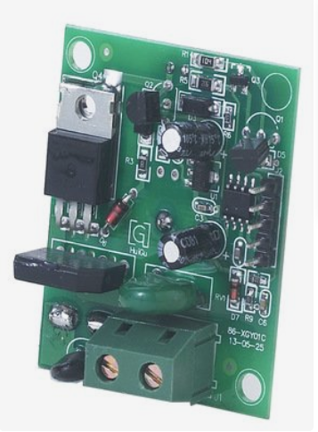


Just upload Gerber files, BOM files and design files, and the KINGFORD team will provide a complete quotation within 24h.