
Professional PCB manufacturing and assembly
Building 6, Zone 3, Yuekang Road,Bao'an District, Shenzhen, China
+86-13410863085Mon.-Sat.08:00-20:00

Organization is the key to design efficiency. Lack of organization will reduce the efficiency of PCB design.
Take design rules as an example: when starting a new project, many PCB engineers tend to re create the design according to their own design rules, rather than relying on an appropriate, organized and systematic rule method.
When the time factor is critical, this approach will greatly reduce the project progress. This paper will discuss the rule method that can improve the design efficiency of multilayer circuit boards.
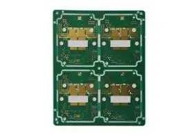
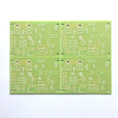
Circuit board design
Consistency and library management
It is common practice to recreate PCB design rules for each new project in progress. This may be because the design department does not have an appropriate process to reuse the rules, or simply because PCB design engineers do not want to reuse these rules.
Whatever the reason, this indicates that the design workflow needs to be updated to improve design efficiency and consistency. Without improvement and promotion, the current workflow may require a lot of additional time and effort, and inconsistency will lead to inheritance problems.
The design rules of each multilayer circuit board are different. In general, we expect PCB design engineers to fully understand the rules and be able to enter the same values in each design. However, even if their memory is correct, there is always the possibility of entering wrong values.
Lack of consistency may eventually lead to different rules controlling multi-layer circuit board components in the whole system. If different circuit boards are used on the same manufacturing panel, this may be a bigger problem. If the structure of one layer is different between different designs, it may lead to manufacturing delay, poor structure or redesign.
In order to simplify the process of creating design rules for multilayer circuit boards, it is better to save and manage these rules for future reuse. The place used to save and manage rules is called "library", which includes schematic symbols, simulation models, design constraints, PCB footprints and STEP models. A library can be as simple as a central file directory for storing data, or it can be a complex system consisting of multiple directory locations and links.
The design rule set can be saved in the same way no matter how the CAD library is set. In order to successfully manage the "library" of design rules, there should be three basic practices in the system:
1. Location: Establish a central location on the server that all users can access. Keep frequently used design rules and other types of data on personal computers for future use. This practice can restrict the access of others, and the saved file is easier to be changed or deleted.
2. Naming convention: name the saved file in a way that is easier for others to recognize. Date, description and job number are good choices for file names. "Joes_really_cool_designe_rules. txt" is not recommended.
3. Limit editing permission: It is better to enable design team members to save their files to this location and then not edit them in this location. Usually, it is very frustrating to suddenly find that the design rules of the six layer circuit board have changed after the last use. At any time, design team members can copy these rules to a new file, make changes, and then name and save them with a new name.
When the design data storage system is in place, it is convenient to use it to save files.
Multilayer board constraints, testing, and system level integrity
Even if only one circuit board is available, signal integrity and power integrity are still key factors to be carefully considered in the design. Compared with today's multi-layer circuit board system, the considerations for a single circuit board are relatively simple: simpler power supply, fewer interference components, and shorter signal transmission distance.
1. System level signal integrity and electromagnetic interference (EMI)
The best way to ensure proper signal integrity (SI) of multilayer circuit boards is to have a reliable and accurate signal integrity analysis and simulation tool to work with the design in each step of the process.
The interaction of high-speed and low-speed signals will certainly cause signal integrity problems, in addition, the possibility of crosstalk with all active components is greater. Therefore, due to the interaction between high-speed signals, multi-layer circuit board design almost always faces greater risk of electromagnetic interference.
By using effective tools or enhancing their functions with our knowledge, separating analog and digital signals, adopting intelligent routing (meaning there is no right angle routing in the circuit) and keeping the signal and return current tightly coupled can significantly reduce the electromagnetic interference problem.
2. Zoning design and cost analysis of multilayer circuit board
Physical grouping of components based on purpose and function can achieve higher security for many factors. This process is called PCB partitioning, and the subsystem can be considered as a group of components in a multi-layer circuit board design.
Proper PCB zoning can simplify operations and improve cost-effectiveness, such as:
Modularization, or integration of standardized components into a larger variety of product designs
Circuit board spacing and actual installation of enclosure circuit
Manufacture cheaper and smaller circuit boards connecting to the motherboard, rather than accessories in the expensive multilayer circuit board stack structure
In multi-layer circuit board design, analog and digital circuits are separated to reduce electromagnetic interference
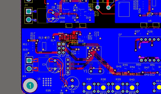
3. PCB constraint manager and multilayer circuit board auxiliary equipment
Although many constraint managers have been equipped with the impedance, stack structure, network and plane selection required to complete the work, an excellent constraint manager will also consider the component list and parameters, which will make the multi-layer circuit board design easier to manage, especially when dealing with thousands of independent components on each circuit board.
The multi-layer circuit board constraint manager can manage advanced network classes, set cooling requirements, quickly adjust cooling specifications under constraints, and process signal conditions.
Multilayer circuit board system architecture and design tools
For the overall integrity of the system, it is important to manage the connectors in the multi-layer circuit board system.
Although we may have made proper planning for everything, when determining the connector suitable for design, it is critical to determine the handling mode of the connector in the enclosure environment, whether to design the vertical or horizontal layering of the circuit board, and potential corrosion (environment, current, electrolysis, etc.).
In the whole PCB layout stage, connectors should be carefully managed. If not fully considered, more attention may be paid to the design rules and constraint manager. When we reroute for a long time without enough energy for final inspection (such as checking the via impedance value), design rule check (DRC) can enable us to clearly see violations and quickly solve problems, rather than just worry and worry.
When design rules were first applied to PCB design tools, their operation was not simple. Users often have to navigate multiple menus and fill in multiple different forms. Usually, the methods used by these systems to save information are not reliable, or even if they are saved, they are only saved in a non formatted text file. However, the times are developing.


Just upload Gerber files, BOM files and design files, and the KINGFORD team will provide a complete quotation within 24h.