
Professional PCB manufacturing and assembly
Building 6, Zone 3, Yuekang Road,Bao'an District, Shenzhen, China
+86-13410863085Mon.-Sat.08:00-20:00

Summarize the process of a single chip microcomputer project development.
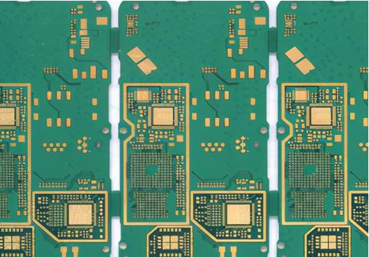
Obviously, to build a single chip project, almost everything is based on the circuit board. The single chip computer and various components are welded on the circuit board, and the program is written in the single chip computer on the circuit board, so the design and production of the circuit board is the basis of the single chip computer project.
Circuit board design process
The first step is to make the process clear. The general process of circuit board design, in fact, circuit board design is not difficult, usually it is to draw the component library of each component to be used (the component library includes the schematic library and packaging library), then draw the schematic diagram, and then generate the first draft of PCB according to the schematic diagram, and then complete the final PCB diagram through layout and wiring. This is the whole design process.
Draw catalogs:
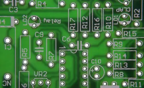
The circuit board design generally includes these elements: components, PCB layout and wiring. The components are the foundation, just like the bricks when we build tall buildings. Without bricks, we can't build a building. Without components, we can't build a circuit board.
protel DXP comes with a part of the component library, but it may not completely cover the design requirements, so you need to design the component library yourself in many cases.
The design of component library includes two aspects: drawing schematic library and packaging library. To do this well, it includes several tasks: drawing schematic symbols of components, component packaging design and binding.
The schematic library is a collection of schematic symbols of each component. The schematic symbols of a component include the name, shape, pin and other information of the component.
Packaging library is a collection of information including the installation and welding of various components on PCB. To put it simply, component packaging is the part of the component that matches the soldering on the circuit board, including elements such as component shape, pads or pads.
Binding means that when the schematic symbols and packages of components are drawn, they need to be bound together so that they can call each other, so that subsequent schematic diagrams and PCB diagrams can be easily drawn in the future.
Draw circuit schematic diagram:
Circuit schematic diagram is a principle level drawing used for better understanding and reading of the whole circuit. Drawing circuit schematic diagram is to organize and draw the hardware required on the circuit board (generally represented by the principle symbols of components) on the diagram according to rules. The schematic diagram is not a real circuit board diagram. For many experts, they may draw PCB drawings without drawing schematic diagrams, but for most developers, schematic diagrams are very meaningful for design and inspection.
Drawing schematic diagram mainly includes several aspects of work, including component placement, component layout, and wiring.
Draw PCB diagram:
The final PCB design still needs to draw a PCB diagram. The PCB diagram is basically the same as the circuit board. The circuit board is made as it is drawn, including the installation shape and position of components, welding pins, wiring between PCB components and other information.
Drawing PCB diagram includes these tasks, including component placement, component layout, and wiring. Here, components refer to component packaging. Many factors need to be considered in component layout, such as the shortest connection, high and low frequency isolation, analog digital isolation, etc., and different line width, line spacing, optimal routing and other factors for different devices need to be considered in connection.
The common circuit board design basically covers these contents, but these works are based on rich knowledge of electrical, analog and digital circuits, which requires time to accumulate.


Just upload Gerber files, BOM files and design files, and the KINGFORD team will provide a complete quotation within 24h.