
Professional PCB manufacturing and assembly
Building 6, Zone 3, Yuekang Road,Bao'an District, Shenzhen, China
+86-13410863085Mon.-Sat.08:00-20:00


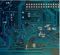
PCB Design of Four layer PCB Process
SMT chip manufacturers introduce PCB design process of circuit boards in detail and the problems that should be noted. In the design process, different layout principles are adopted for common components and some special components; Compare the advantages and disadvantages of manual wiring, automatic wiring and interactive wiring; This paper introduces PCB circuit and relevant measures to reduce interference between circuits. Combined with personal design experience, taking the PCB design of the core board of embedded system based on ARM and autonomous mobile as an example, this paper briefly introduces the PCB design process of the four layer circuit board and related issues that should be noted.
Printed circuit board (PCB) plays the role of supporting circuit components and devices in electronic products, and also provides electrical connection between circuit components and devices. In fact, PCB design is not only simple to arrange and fix components, but also to connect the pins of components. Its quality has a great impact on the anti-interference ability of products, and even plays a decisive role in the performance of products in the future. With the rapid development of electronic technology, the overall dimensions of components and products are becoming smaller and smaller, and the working frequency is getting higher and higher, which greatly increases the density of components on PCB, which also increases the difficulty of PCB design and processing. Therefore, it can be said that PCB design is always one of the most important contents in the development and design of electronic products. 1 Layout The so-called layout is to reasonably arrange all components in the circuit diagram on a PCB with limited area. From the signal point of view, there are mainly three kinds of digital signal circuit board, analog signal circuit board and mixed signal circuit board. When designing the mixed signal circuit board, it is necessary to carefully consider, and place the components in the proper position of the circuit board by hand, so as to separate the digital and analog components, as shown in Figure 1.
In the process of arranging PCB layout, the most critical problem is: switches, buttons, knobs and other operating parts as well as structural parts (referred to as "special components") must be arranged to the designated (appropriate) positions in advance. After placement, you can set the attributes of the components and select LOCK to prevent them from being moved by mistake in future operations; For the location arrangement of other components, it is necessary to take into account the optimization of wiring distribution rate and electrical performance, as well as the future production process and cost and other factors. The so-called "consideration" is often a challenge to the level and experience of the design staff.
1.1 Layout principle of special components ① The connection between components shall be shortened as much as possible to reduce their distribution parameters and mutual electromagnetic interference. Those components susceptible to electromagnetic interference should not be too close, and input and output components should be as far away from each other as possible.
② There may be high potential difference between some components or wires, so the distance between them should be increased to avoid accidental short circuit caused by discharge; At the same time, from the perspective of safety, the components with high voltage should be arranged in places that are not easily accessible during commissioning. ③ Large devices with a mass of more than 15g shall be fixed with brackets before welding. Those large, heavy and heat generating components should not be installed on the printed board, but should be installed on the chassis of the whole machine; In addition, heat dissipation shall be considered. Thermal components shall be far away from heating components (except those used for over temperature protection). ④ For the layout of adjustable components such as adjustable potentiometers, inductors, variable capacitors, microswitches, etc., the structural requirements of the whole machine shall be considered. If it is adjusted in the machine, it should be placed on the printed board where it is convenient for adjustment; If it is adjusted outside the machine, its position shall be consistent with the position of the adjustment knob on the chassis panel.
1.2 Layout of common components ① Arrange the position of each circuit unit according to the circuit flow, so that the layout is convenient for the flow of signals, and the signals can be kept in the same direction as far as possible. ② Take the core components of each functional circuit as the center, and arrange around it. The components shall be evenly, neatly and compactly arranged on the PCB, and the leads and connections between components shall be minimized and shortened. ③ For circuits operating at high frequencies, the distribution parameters between components should be considered. In general, the circuit should be arranged in parallel as far as possible, which can not only achieve aesthetic effect, but also be easy to assemble, weld and mass produce. ④ Components located at the edge of the circuit board are generally not less than 2mm away from the edge of the circuit board; The best shape of the circuit board is rectangle, and its aspect ratio can be 3:2 or 4:3. When the size of circuit board is greater than 200mm × For 150mm, the mechanical strength of the circuit board shall be considered. In the actual design process, if the required size of the PCB cannot be determined at the beginning, it can be slightly larger. After PCB design, select Design → Board Shape → Redefine Board Shape in Protel DXP to cut the original PCB properly.
In addition, according to my actual work experience, if you want to expand or reduce some functions of the existing circuit board, and need to redesign a new PCB, you can refer to the layout on the motherboard in the actual layout, and manually arrange the components in the appropriate position; In the wiring process, adjust according to the actual needs to further improve the routing rate.
2. After the layout, all the wiring is connected according to the schematic diagram through the wiring diagram of copper foil. Obviously, the rationality of the layout will directly affect the success rate of the routing, so it is often necessary to adjust the layout properly in the entire routing process. Wiring design can adopt double-layer wiring and single-layer wiring; For extremely complex designs, multi-layer cabling can also be considered.
In PCB design, wiring is an important step to complete product design. It can be said that all the previous preparations were made for it. PCB wiring includes single-sided wiring, double-sided wiring and multi-layer wiring. There are two ways of routing: automatic routing and interactive routing.
In PCB design, designers often hope to use automatic wiring. In general, it is no problem to use automatic wiring for pure digital signal circuit boards (especially when the signal level is relatively low and the circuit board density is relatively small). However, when designing analog signals, mixed signals or high-speed circuit boards, if automatic wiring is also fully used, there will be problems, even serious circuit performance problems.
At present, although some automatic routing tools have very powerful functions, which can usually reach 100% of the routing rate, the overall appearance is not very beautiful. Sometimes the wiring is arranged in disorder, and the wiring between two pins is not the shortest (optimal) path. For the relatively complex circuit design, please try not to completely adopt the automatic wiring mode. It is recommended that the wires with strict requirements should be routed interactively in advance before automatic routing is adopted. At the same time, the side lines of the input and output terminals shall not be adjacent and parallel to avoid reflection interference; The wiring of two adjacent layers should be perpendicular to each other, and parallelism is prone to parasitic coupling. This constraint can be added in the wiring rules. The routing rate of automatic routing depends on good layout. The routing rules should be preset, including the number of bending times of routing, the number of through holes and the number of steps. Generally, the exploratory market line is carried out first, and the short line is quickly connected first; Then perform maze routing. First, optimize the global routing path of the lines to be routed. It can disconnect the already routed lines as needed and re route them to improve the overall effect. In manual wiring, in order to ensure the correct implementation of the circuit, we need to follow some general design rules: try to use the ground plane as the current loop; Separate the analog ground plane from the digital ground plane; If the ground plane is separated by the signal line, the signal line shall be perpendicular to the ground plane to reduce the interference to the ground current loop; The analog circuit shall be placed as close as possible to the edge of the circuit board, and the digital circuit shall be placed as close as possible to the power connection end, so as to reduce the di/dt output effect caused by the digital switch.
3 PCB circuit and circuit anti-interference measures The anti-interference design is closely related to the specific circuit, and it is also a very complex technical problem. Here is a brief introduction based on the experience in PCB design. ① Design of power cord. According to the size of PCB current, the width of the power line should be thickened as much as possible (in the wiring design rules, a new constraint rule can be made for the line width of the power line and ground line separately) to reduce the loop resistance. In particular, it should be noted that the power supply direction of the power line and ground line is opposite to the transmission direction of data and signal, which is helpful to enhance the anti noise ability. ② Design of ground wire. The ground wire is not only a special power line, but also a signal line. In addition to following the design principles of the power cord, it should also be: digital and analog are separated; If there are both logic circuits and linear circuits on the circuit board, they should be separated as far as possible; The grounding of low-frequency circuit shall be single point parallel grounding as far as possible. If the actual wiring is difficult, part of the circuit can be connected in series and then connected to the ground in parallel; High frequency circuit should adopt multipoint series grounding, the ground wire should be short and thick, and the grid shape should be used for large area copper coating around high-frequency components as far as possible; The width of power supply and ground wire should be widened as much as possible. The ground wire should be wider than the power line. Their width relationship is: ground wire>power line>signal line. ③ The grounding of digital circuit system constitutes a closed loop, that is, a grounding grid, which can improve the anti noise ability. ④ Digital current shall not flow through the simulator, and high-speed current shall not flow through low-speed devices. ⑤ A coupling capacitor is added between the power supply ground wires to improve the anti-interference capability of the power supply circuit.
4 Specific Example The following example is the PCB design of the core board of the embedded system based on ARM and autonomous mobility.
4.1 Core board schematic diagram In the core board schematic diagram, the core component is S3C44BOX. This component is a high-performance 16/32 bit RISC microprocessor, with the main frequency of 66MHz. It is internally integrated with a LCD controller, suitable for handheld devices, and packaged with 160-QFP. In this system, 5V and 3.3V DC regulated power supplies are required for the power circuit, among which, 2.5V power supplies are used for S3C44BOX, 3.3V power supplies are required for peripheral devices, and 5V power supplies are required for other devices; The crystal oscillator circuit is used to provide the working clock to the CPU and other circuits, and the S3C44BOX uses the commonly used passive crystal oscillator; U6, U7 and U9 constitute the storage system of this system.
4.2 Four layer circuit board wiring rules ① The software tool used in this PCB design is Protel DXP. The core board is a four layer circuit board, the top layer and bottom layer are signal layers, and the middle two layers are power layer and layer respectively.
② The original PCB size of the motherboard is 55mm × 70mm, but in the actual design process, if the PCB size is also designed to this value, it will encounter practical difficulties in the wiring process, so first design the board size to be slightly larger. After the wiring is successful, select Design → Board Shape → Redefine Road Shape to cut the PCB board. ③ When generating PCB drawings from schematic diagrams, manually place some strict components (U5, U6, U7 and U9) at appropriate positions and lock them; At the same time, place the crystal oscillator near U5. When placing other components, pay attention to the distance between the components. If the two components are too close, interference will occur, and it will be displayed in green. ④ In the system, the on-chip operating frequency of S3C44BOX is 66MHz. Therefore, in the process of PCB design, some basic principles of high-frequency circuit design should be followed, otherwise the system will not work stably or even normally. ⑤ For the current high-density PCB design, it has been felt that the through-hole is not suitable, wasting many valuable wiring channels. In order to solve this contradiction, blind hole and buried hole technology emerged, which not only realized the role of through hole, but also saved many wiring channels, making the wiring process more convenient, smooth and perfect. In most of the courses, blind hole and buried hole techniques are also advocated in the design of multilayer circuit boards. Although this can make the wiring work easier, it also increases the cost of PCB design. Therefore, whether to select this technology depends on the actual circuit complexity and economic capacity. The author did not use this technology in the process of designing the four layer board. If the number of through holes is too large, the upper limit of drilling can be limited in the wiring rules before wiring. ⑥ Before wiring, the top layer uses horizontal wiring and the bottom layer uses vertical wiring in the wiring rules. In this way, the top layer and bottom layer can be perpendicular to each other to avoid parasitic coupling; At the same time, the right angle or acute angle shall be avoided at the corner of the connection between the pins, because they will affect the electrical performance in the high-frequency circuit. ⑦ PCB design adopts interactive wiring mode. First, manually pre wire the pin connections between components J1, J2 and U5. In the input/output signals of the microprocessor, there are quite a few of the same types, such as data lines, address lines and signal lines. These signal wires of the same type should be grouped and distributed in parallel, and the length difference between them should not be too large, which can not only reduce interference and enhance the stability of the system, but also make the wiring simple and the appearance of the printed circuit board more neat and beautiful. Then the rest of the components are automatically routed (different routing strategies can be tried). When the routing is successful, some undesirable routing can be modified and optimized. ⑧ After the wiring design is completed, carefully check whether the wiring design conforms to the rules formulated by the designer, and confirm whether the rules formulated conform to the requirements of the PCB production process; Then, the pad shall be filled with tears, so that the pad is not easy to peel and the wiring is not easy to disconnect from the pad; Finally, a large area of copper is coated on the printed circuit board, which is conducive to heat dissipation, shielding and interference reduction. As the adhesive between the base plate of printed circuit board and copper foil will produce volatile gas that cannot be eliminated when it is immersed or heated for a long time, and the heat is not easy to be dissipated, resulting in the phenomenon of copper foil expansion and falling off, when it is laid in a large area, its opening window should be designed as a mesh.
PCB process High speed PCB wiring attention
Oct 30,2022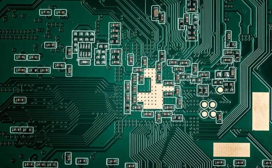


Just upload Gerber files, BOM files and design files, and the KINGFORD team will provide a complete quotation within 24h.