
Professional PCB manufacturing and assembly
Building 6, Zone 3, Yuekang Road,Bao'an District, Shenzhen, China
+86-13410863085Mon.-Sat.08:00-20:00

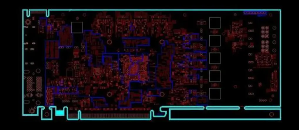
We usually encounter various problems with safe spacing, such as the spacing between vias and pads, the spacing between PCB routing and routing, and so on. Today, we will divide these spacing requirements into two categories: electrical safety spacing; The other is non electrical safety distance.
Electrical safety distance:
1. Spacing between conductors:
According to the production capacity, the distance between the lines shall not be less than 4 MIL. Line spacing is also line to line and line to pad spacing. From the perspective of our production, of course, the bigger the better if conditions permit. Generally, 10 MILs are common.
2. PCB pad aperture and pad width:
According to the PCB manufacturer, if the pad hole diameter is mechanically drilled, it shall not be less than 0.2mm, and if it is laser drilled, it shall not be less than 4mil. The hole diameter tolerance varies slightly depending on the plate. Generally, it can be controlled within 0.05mm. The pad width shall not be less than 0.2mm.
PCB design manufacturer
3. Spacing between pads:
According to the processing capacity of PCB manufacturer, the distance between pads shall not be less than 0.2MM.
4. Spacing between copper sheet and plate edge:
The distance between the electrified copper sheet and the PCB board edge shall not be less than 0.3mm. In case of large area copper laying, it is generally required to have an inside distance with the board edge, which is generally set as 20mil. In general, for the mechanical consideration of the finished circuit board, or to avoid the curling or electrical short circuit caused by the exposure of the copper sheet on the board edge, the engineer often shrinks the large area of copper paving block by 20 mils relative to the board edge, instead of laying the copper sheet to the board edge all the time. There are many ways to deal with the copper skin shrinkage. For example, draw a keepout layer on the board edge, and then set the distance between copper paving and keepout.
Non electrical safety distance:
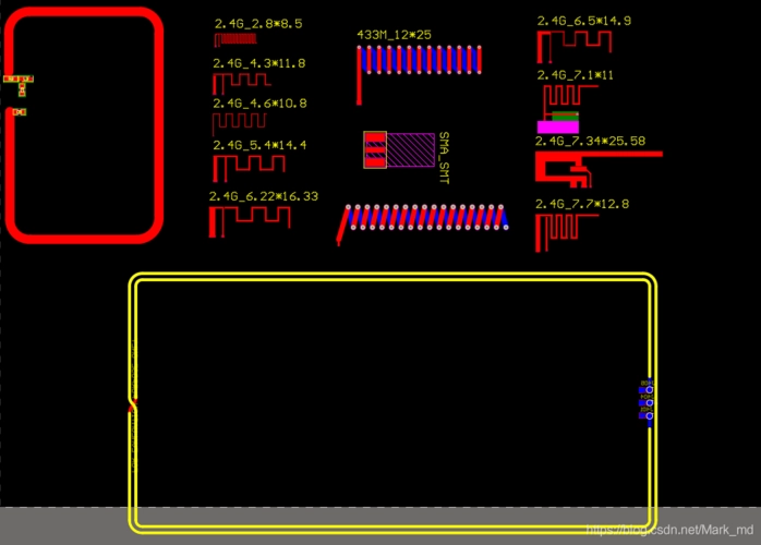
1. Width, height and spacing of characters:
For silk screen characters, we generally use the conventional values, such as 5/30 6/36 MIL. Because when the text is too small, the processing and printing will be blurred.
2. Distance from PCB screen to bonding pad:
Screen printing is not allowed to mount pads. Because if the solder pad is covered with the silk screen, the silk screen cannot be coated with tin, which affects the assembly of components. Generally, 8mil spacing is required to be reserved in PCB factory. If it is because the area of some PCB boards is very close, the spacing of 4MIL is also acceptable. If the silk screen accidentally covers the bonding pad during design, the board factory will automatically eliminate the silk screen left on the bonding pad during manufacturing to ensure tin on the bonding pad. So we need to pay attention.
3. 3D height and horizontal spacing on mechanical structure:
When mounting PCB components, it is necessary to consider whether the horizontal direction and space height will conflict with other mechanical structures. Therefore, in the design, it is necessary to fully consider the adaptability of space structure between components, as well as between PCB finished products and product shells, and reserve a safe space for each target object.


Just upload Gerber files, BOM files and design files, and the KINGFORD team will provide a complete quotation within 24h.