
Professional PCB manufacturing and assembly
Building 6, Zone 3, Yuekang Road,Bao'an District, Shenzhen, China
+86-13410863085Mon.-Sat.08:00-20:00

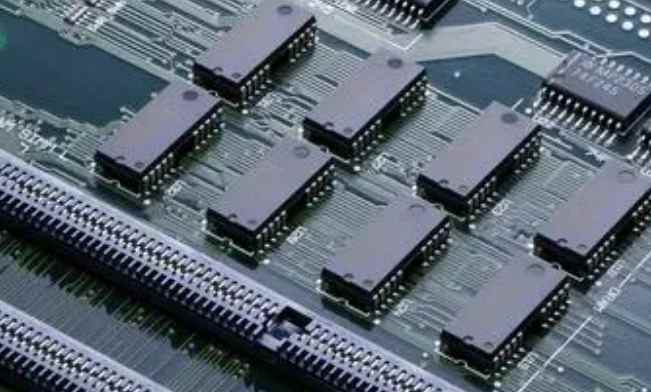
Reviewing the process development of electronics industry in recent years, we can notice an obvious trend is reflow welding technology. In principle, the reflow process can also be used for conventional inserts, which is commonly referred to as through-hole reflow welding. The advantage is that it is possible to complete all the solder joints at the same time, so that the production cost is minimized. However, temperature sensitive components limit the application of reflow welding, both in cartridge and SMD. Then people turned their attention to selective welding. Selective welding can be used after reflow welding in most applications. This will be an economical and efficient method of welding the remaining inserts and is fully compatible with future lead-free welds.
Process characteristics of selective welding
The process characteristics of selective welding can be understood by comparing with wave soldering. The most obvious difference between the two is that in wave soldering, the lower part of the PCB is completely immersed in the liquid solder, whereas in selective welding, only certain areas are in contact with the solder wave. Since PCB itself is a poor heat transfer medium, it will not heat and melt the solder joints near the components and PCB area during welding. Flux must also be pre-applied before welding. In contrast to wave soldering, the flux is only applied to the lower part of the PCB to be soldered, not the entire PCB. In addition, selective welding is only applicable to the welding of cartridge components. Selective welding is a completely new method. A thorough understanding of selective welding process and equipment is necessary for successful welding.
Selective welding process

Typical selective welding processes include flux spraying, PCB preheating, dipping, and drag welding.
Flux coating process
Flux coating process plays an important role in selective welding. At the end of welding heating and welding, the flux should be sufficiently active to prevent bridging and prevent PCB oxidation. Flux spraying The PCB is carried by the X/Y manipulator through the flux nozzle, and the flux is sprayed on the PCB to be welded. The flux can be sprayed by single nozzle spray, microporous spray and synchronous multi-point/graphic spray. The most important thing for microwave peak selective welding after reflow welding process is accurate spraying of flux. Microjet will never stain the area outside the solder joint. The minimum flux spot graphic diameter of micro-dot spraying is greater than 2mm, so the flux position accuracy of spraying deposited on the PCB is ±0.5mm, so as to ensure that the flux is always covered on the welding site. The tolerance of spraying flux quantity is provided by the supplier, and the technical specification should specify the flux usage, usually 100% safety tolerance range is recommended.
Preheating process
The primary purpose of preheating in the selective welding process is not to reduce thermal stress, but to remove the solvent predrying flux, so that the flux has the correct viscosity before entering the solder wave. During welding, the influence of heat brought by preheating on welding quality is not the key factor. PCB material thickness, device package specification and flux type determine the setting of preheating temperature. In selective welding, there are different theories about preheating: some process engineers think that PCB should be preheated before flux spraying; Another view is to weld directly without preheating. Users can arrange the selective welding process according to the specific situation.
Welding technology
There are two different selective welding processes: drag welding and dip welding.
The selective drag welding process is performed on a single small nozzle solder wave. The drag welding process is suitable for welding in very tight Spaces on PCBS. For example: individual solder joints or pins, a single row of pins can be used for drag welding process. The PCB moves on the solder wave of the solder nozzle at different speeds and angles to achieve the best welding quality. To ensure the stability of the welding process, the inner diameter of the welding nozzle is less than 6mm. After the flow direction of the solder solution is determined, the solder nozzle is installed and optimized in different directions for different welding needs. The manipulator can approach the solder wave from different directions, that is, 0° ~ 12° at different angles, so the user can weld various devices on the electronic components. For most devices, the recommended inclination Angle is 10°.
Compared with the dip welding process, the motion of solder solution and PCB board in the drag welding process makes the thermal conversion efficiency better than that in the dip welding process. However, the heat required to form the weld connection is transferred by the solder wave, but the solder wave quality of single nozzle is small, only the solder wave temperature is relatively high, to meet the requirements of the drag welding process. Example: Solder temperature is 275℃ ~ 300℃, drag speed of 10mm/s ~ 25mm/s is usually acceptable. Nitrogen is supplied in the welding area to prevent oxidation of solder wave, which eliminates oxidation and avoids the generation of bridge defects in the tow welding process. This advantage increases the stability and reliability of the tow welding process.
PCB through hole technology is fully introduced
Apr 19,2023


Just upload Gerber files, BOM files and design files, and the KINGFORD team will provide a complete quotation within 24h.