
Professional PCB manufacturing and assembly
Building 6, Zone 3, Yuekang Road,Bao'an District, Shenzhen, China
+86-13410863085Mon.-Sat.08:00-20:00


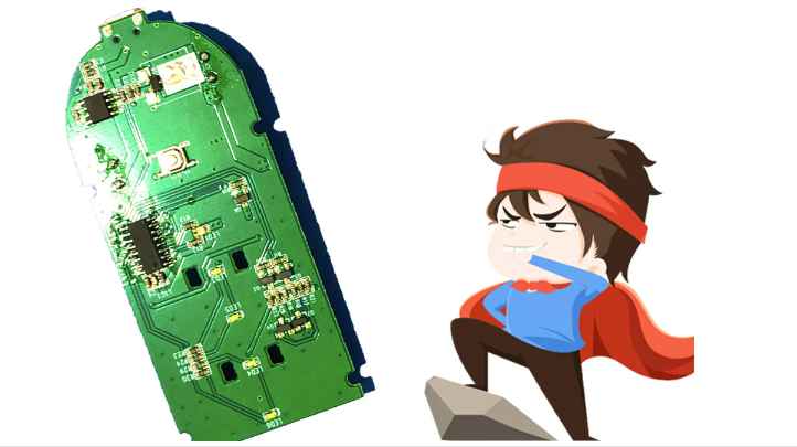
Don't think PCB board is very simple, it can only show that your level still needs to be improved. With the increasing density of modern integrated devices, the quality of PCB layout directly affects the performance of products, and even the key to the success or failure of design.
1, schematic diagram to facilitate wiring, troubleshooting as the principle, reasonable use of the bus, the use of real pin distribution;
2. Before PCB generation, all the sparse devices should be manually packaged, and triode packaging should be prepared in advance;
3. Before wiring, a manual drawing should be carried out, and the general layout should be carried out under the principle of performance priority;
4. Avoid parallel wiring with the axis of components, carefully set the ground wire, and properly use comprehensive or grid copper covering;
5, the ground wire in the digital circuit should be a network, the reasonable use of signal clock line snake line, welding plate should be appropriate;
6, the manual wiring should be wired according to the network or components, and then the docking and arrangement between the blocks;
7, layout emergency modification, must be calm, generally only need to change individual components or one or two networks.
8. When making PCB, at least five welding holes, four corners and center should be set aside in the blank for hole matching;
9, before welding, it is best to brush tin, components on the board first, with tape fixed after welding;
10. ADC circuit routing shall be separated from other digital circuits or signal lines (especially clock) routing. Parallel and crossing is strictly prohibited;

11. The oscillating crystal should be as short as possible and surrounded by ground wire, but note that the load capacitance cannot be increased due to too small spacing;
12, single and double panels should have at least 50% of the metal layer, multilayer at least four layers of metal layer, to prevent local overheating and fire;
13, the signal cable as far as possible the thickness is consistent and short, signal cable, input and output lines to add ground wire, between the modules should also clip ground wire;
14, device pin and ground contact is best not large area covered with copper, and with grid, the whole plate covered with copper to prevent skin also with grid;
15. If a large area of copper is covered on the PCB board, several small openings should be made on the ground, but the holes should not be larger than 3.5mm, which is equivalent to the grid;
16, in order to avoid too long cable and use jumper, jumper should not be placed under the IC integrated block and other large devices, in order to facilitate plugging;
17, layout wiring should fully consider the heat dissipation and ventilation of the device, the heat source should be close to the edge of the plate, and design a good distance between the test points;
18. 20H rule and 3W rule should be applied in the design of multi-layer anti-electromagnetic interference to overcome boundary radiation coupling and logical current flux interference;
19, double signal line should not be the same direction of the current, and to control the minimum parallel length, such as JOG line or sine, cosine line;
20. The interference brought by the change of signal up and down the low frequency line is far greater than the interference generated by the frequency, so we should also pay attention to the crosstalk problem;
21, high-speed signal line to join the appropriate end matching, and it is best to keep its impedance in transmission remains unchanged, and try to widen the width of the line; Bioneng belongs to Qinji Group, is the leading electronic industry service platform in China, providing online components, sensor procurement, PCB customization, BOM, material selection and other electronic industry supply chain solutions, one-stop to meet the comprehensive needs of small and medium-sized customers in the electronics industry.
22. When exporting and exporting the data files of PCB welding holes and holes, the layout printed by the CNC machine tool is reversed or mirrored with the layout displayed in the computer. That is: the actual out of the board is the circuit diagram to the right edge line as the reference line to the right after 180 degrees of the page. Pay special attention when there is a blank space! Otherwise the board is useless!
In the production of PCB single panel, you can use three or five point positioning method for board holes, you can also transfer ink paper to the copper-covered plate, and then use 0,0 points or add a diagonal point method to make NC machine automatically positioned on the above hole. But because it is the naked eye to the reference coordinate point, so a little mistake may lead to all the holes are not accurate.


Just upload Gerber files, BOM files and design files, and the KINGFORD team will provide a complete quotation within 24h.