
Professional PCB manufacturing and assembly
Building 6, Zone 3, Yuekang Road,Bao'an District, Shenzhen, China
+86-13410863085Mon.-Sat.08:00-20:00

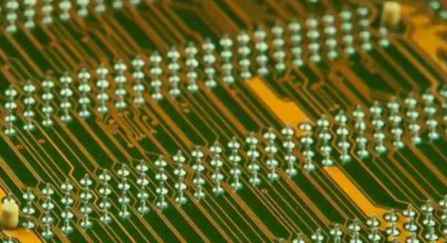
With the rapid development of electronic technology and the wide application of wireless communication technology in various fields, high frequency, high speed and high density have gradually become one of the obvious development trends of modern electronic products. The high frequency and high speed digitalization of signal transmission force PCB to move towards micro hole and buried/blind hole, wire fine, medium layer uniform thin shape. The design technology of high frequency, high speed and high density multi-layer PCB has become an important research field. Elaborated PCB design high frequency circuit board wiring skills, specific follow Xiaobian together to understand.
PCB design high frequency circuit board wiring skills
First, the less the lead bending between the pins of high-speed electronic components, the better
It is better for the wiring of high frequency circuit to adopt full straight line, which needs a turn, which can be used as a 45 degree fold line or arc turn. This requirement is only used to improve the fixation strength of copper foil in low frequency circuit, and in high frequency circuit, meeting this requirement can reduce the external transmission of high frequency signals and the coupling between each other.
Two, high-frequency circuit device pin between the lead layer alternations less, the better
The phrase "the less interlayer alternations of leads, the better" means that the fewer holes (Via) used in the connection of components are the better. A single pass hole brings about 0.5pF of distributed capacitance, and reducing the number of pass holes significantly increases speed and reduces the possibility of data errors.
Three, the shorter the lead between the pin of the high-frequency circuit device, the better
The radiation intensity of the signal is proportional to the length of the signal line. The longer the high-frequency signal lead, the easier it is to be coupled to the components close to it. Therefore, for high frequency signal lines such as signal clock, crystal oscillator, DDR data, LVDS wire, USB cable, HDMI cable, etc., the shorter the cable is required as far as possible.
Four, the integrated circuit block power pin increase the high frequency of the lotus root capacitance
Each integrated circuit block power pin to add a high frequency dropout capacitor. Increasing the high frequency decoupling capacitance of the power supply pin can effectively compress the high frequency harmonics on the power supply pin to form interference.
5. Avoid the loop formed by cable routing
All kinds of high-frequency signals should not form a loop. If it cannot be avoided, the loop area should be as small as possible. Bioneng belongs to Qinji Group, is the leading electronic industry service platform in China, providing online components, sensor procurement, PCB customization, BOM, material selection and other electronic industry supply chain solutions, one-stop to meet all the needs of small and medium-sized customers in the electronics industry.

Six, high frequency digital signal ground and analog signal ground to do isolation
When analog ground wire and digital ground wire are connected to the public ground wire, high frequency choke magnetic beads should be used to connect or directly isolate and select the appropriate ground single point interconnection. The ground potential of ground wires of high frequency digital signals is generally inconsistent, and there is often a certain voltage difference between the two directly. Moreover, ground wires of high frequency digital signals are often rich in harmonic components of high frequency signals. When the ground wires of digital signals and analog signal ground wires are directly connected, the harmonics of high frequency signals will interfere with analog signals by means of ground wire coupling. Therefore, under normal circumstances, the ground wire of the high frequency digital signal and the ground wire of the analog signal should be isolated, which can be used in the way of single point interconnection at the appropriate position, or the way of high frequency choke magnetic bead interconnection.
7. Pay attention to "crosstalk" introduced by short distance parallel running of signal line
High frequency circuit wiring should pay attention to "crosstalk" caused by short distance parallel routing of signal lines. Crosstalk refers to the coupling phenomenon between signal lines that are not directly connected. Since high-frequency signals are transmitted along the transmission line in the form of electromagnetic waves, signal lines will play the role of antennas, and the energy of electromagnetic fields will be transmitted around the transmission line. The unwanted noise signals generated between signals due to the mutual coupling of electromagnetic fields are called Crosstalk. The parameters of PCB board layer, the distance between signal wires, the electrical characteristics of the driver and receiver end, and the connection mode of signal wires all have a certain influence on the crosstalk. So in order to reduce the crosstalk of high frequency signals, the following points should be done as far as possible when wiring:
1. If parallel cabling in the same floor is almost unavoidable, the direction of the two adjacent floors must be perpendicular to each other;
2. If the wiring space allows, insert a ground wire or ground plane between two lines with more serious crosstalk, which can play the role of isolation and reduce crosstalk;
3. When time-varying electromagnetic fields exist in the space around the signal line, if parallel distribution cannot be avoided, a large area of "ground" can be arranged on the opposite side of the parallel signal line to greatly reduce interference;
4. In digital circuits, the usual clock signals are signals with fast edge changes and large external crosstalk. Therefore, in the design, the clock line should be surrounded by the ground line and more ground holes to reduce the distributed capacitance, so as to reduce crosstalk;
5. For the high frequency signal clock, try to use the low voltage differential clock signal and include the ground, and pay attention to the integrity of the ground punching;
6, under the premise of wiring space permit, increase the spacing between adjacent signal lines, reduce the parallel length of signal lines, clock line and the key signal line as far as possible vertical rather than parallel;
7. The idle input terminal should not be suspended, but grounded or connected to the power supply (the power supply is also ground in the high-frequency signal loop), because the suspended line may be equivalent to the transmitting antenna, and the grounding can press the transmission. Eliminating crosstalk in this way has sometimes proved to be effective immediately.
Review according to the "PCB checklist
Apr 02,2023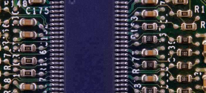


Just upload Gerber files, BOM files and design files, and the KINGFORD team will provide a complete quotation within 24h.