
Professional PCB manufacturing and assembly
Building 6, Zone 3, Yuekang Road,Bao'an District, Shenzhen, China
+86-13410863085Mon.-Sat.08:00-20:00

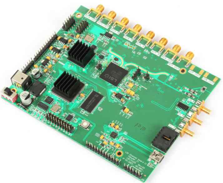
PCB board is a problem that needs to be dealt with in the process of PCBA processing. When the PCB design engineer has determined the shape of the PCB, the circuit board can be pieced design. For most circuit boards, the assembled board can improve production efficiency and reduce plate loss. Since the Mosaic has so many benefits, then how to set the number of PCBA processing, need to consider what factors? The following PCBA processing manufacturer Xiaobian to explain how to set the number of PCB pieces and how to solve the SMT patch processing tablet problem related knowledge.
1. How to solve the SMT patch processing tablet problem
In the SMT patch processing process, sometimes there will be chip components stand up phenomenon, commonly known as the monument. This is a phenomenon of poor PCBA processing, which requires PCBA processing manufacturers to find out the reason and solve the problem. Then what factors will lead to SMT patch processing monument, how to solve the SMT patch processing monument problem, the next Shenzhen -kingford for you to introducPCBA processing manufacturere. The root cause of the stele phenomenon is that the welding tension on both sides of the component is not balanced, which causes the degree of wetting at both ends of the component is not balanced. The following situations will cause uneven wetting force at both ends of components during reflow welding during SMT patch processing, resulting in the phenomenon of stellage.
First, the PCB design problem
A. The size design of the pad is irregular. For example, the pad at both ends of the component is usually too large on one side of the pad connected with the ground wire, and the heat capacity at both ends of the pad is uneven. Of course, if the manufacturing process level of PCB board factory is too poor, similar problems will also occur.
b. The size difference of the pad leads to different solder paste dissolution welding forces, resulting in a saw-saw state at both ends of the pad in the welding process.
c. Improper layout of components. The temperature difference in PCB board is too large to cause uneven heat absorption on both sides of the component pad, such as: special-shaped devices, structural parts, QFP, BGA, large heat-absorbing devices around the small chip components at both ends of the pad will appear uneven temperature, then the solder paste dissolution caused by the welding tension imbalance.
d. Unreasonable inner distance of welding disc.

2. How to set the number of PCB fragments
Next, kingford, PCBA processing manufacturer, will introduce it to you. There are many ways of circuit board, such as two in one, three in one, four in one, it is more common to more than two pieces of the same circuit board into a large circuit board; With different shapes of the circuit board can also be pieced together, but the application is less, mainly when the number of different shapes of the board is difficult to match; Yin and Yang board is the same kind of circuit board positive and negative sides of a circuit board, Yin and Yang board can improve SMT processing efficiency, suitable for a small number of components of the circuit board.
Yin and Yang board design is not suitable for all circuit boards, if a side of the circuit board concentrated design of the heavier components, the use of Yin and Yang board is likely to lead to the surface as a second hit when the heavier parts fall. There is a large area of heat-absorbing components on the board can not use the Yin and Yang board design. The disadvantage of Yin and Yang plate is that SMT processing is limited, which is easy to cause uneven heating phenomenon. The specific use of which kind of board way or comprehensive consideration of various factors. The cost of board making is the most important factor to measure the number of board making. Circuit board manufacturers in order to improve production efficiency and reduce costs will have a basic standard board size, these standards repeatedly consider the board board optimal utilization. Common standards are 16.16 "x16.16," 18.32 "x18.32", 20.32 "x20.32",... Etc. The cost of the circuit board will be affected by the size of the board, choose the most appropriate standard board, achieve the optimal board utilization rate can reduce the production cost of the circuit board. The cost of the circuit board is also related to the number of layers of the board, the number of holes, and whether there are blind holes and other factors.
The SMT machining line is divided into long line and short line according to the different use requirements. The short line has at most two fast laminator and one slow laminator; A long line usually has multiple fast and slow SMT machines. Usually, each line is equipped with a solder paste press, and it takes about 35-40 seconds to brush the solder paste for a 150mm piece of board. In SMT short line processing, the time allocated for each machine is about 10-26 seconds, and the time allocated for the SMT paste printing is much lower than that for the solder paste printing, indicating that the SMT machine is waiting for the solder paste printing machine and does not make full use of the capacity of the SMT machine. Switching from two-in-one to four-in-one results in an immediate efficiency boost (output per hour), as shown in the chart below: 2 in 1 board solder paste printing (s) Fast machine one (s) Fast machine two (s) Slow machine (s) Bottleneck time (s) Every hour output Top3826261038188 Bottom4034352440180 pieces 4 in 1 board solder paste printing (s) Fast machine one (s) Fast machine two (s) Slow machine (s) Bottleneck time (s) per hour output Top3852522052276 Bottom4068704870204 tablets Note: Output per hour ={[60(seconds/minute) x 60(minutes/hour)] / Bottleneck time (seconds)} x number of pieces. In conclusion, PCB manufacturers usually hope that the fewer the number of boards, the better, because the fewer the number of boards, the less the probability of X board, which can reduce the scrap rate and reduce the cost of board making. SMT factories also do not like to make X plates, because it will reduce the efficiency of processing. Therefore, it is still necessary to calculate the most affordable number of panels from the perspective of the overall PCBA processing cost. The process capacity of PCB and SMT factories also has an impact on this. Also consider whether to use V-cut or Router process to edge the board, which will also affect the board design.
How to improve the PCB short-circuit problem
Feb 05,2023


Just upload Gerber files, BOM files and design files, and the KINGFORD team will provide a complete quotation within 24h.