
Professional PCB manufacturing and assembly
Building 6, Zone 3, Yuekang Road,Bao'an District, Shenzhen, China
+86-13410863085Mon.-Sat.08:00-20:00

The significance of SMT processing and its processing and desoldering
What is the meaning of SMT patch processing?
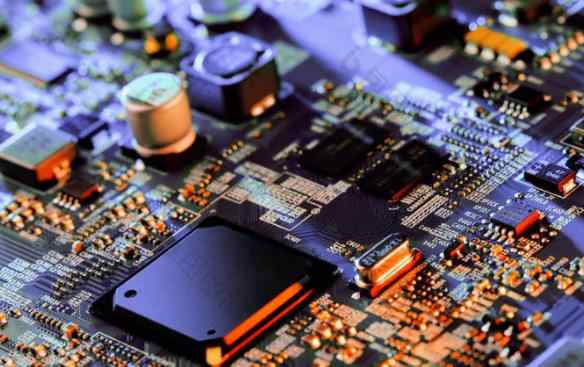
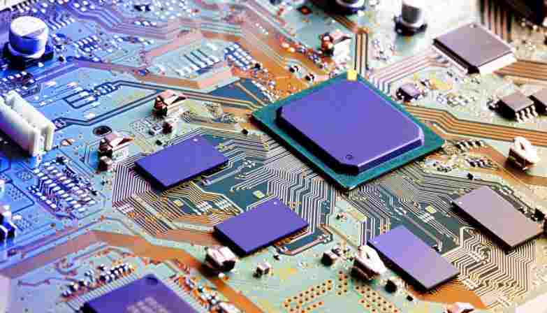
The meaning of SMT chip processing is to install and weld the required chip components to the fixed position on the printed circuit board SMT refers to surface mount technology, which is very popular in the electronic processing industry The data used for SMT chip processing technology mainly include the following contents: flux, solder paste, patch glue, etc Solder paste is a kind of solder paste used for reflow soldering process Now SMT wafer processing plants use solder paste, and the main method used is template omitting printing This method has the advantages of easy operation, unstable reliability and high cost
The patch adhesive is heated and cured at 150 ℃. Select the type of paster according to different printed circuit boards. Flux is usually used together with tin powder, and sometimes some solvents are added to expand the effect of the activator. The composition of the flux determines the wettability, viscosity change, storage life, expansibility, collapse and cleanliness of the solder paste. PCB design is closely related to SMT chip processing. If the PCB is not designed properly, it will cause waste of man hours, data and components, resulting in heavy losses.
The cost of SMT chip processing consists of several parts. One is the material cost, including auxiliary material cost, direct material cost, etc First, manufacturing and labor costs, including management salaries, depreciation expenses, ordinary workers' salaries, utilities, rents, etc The equipment used for SMT placement processing includes high-speed placement machine, multi-function placement machine, solder paste printer, solder paste mixer, etc Cheap equipment costs tens of thousands of yuan, while expensive equipment costs millions of yuan
The products that can be processed with SMT include wireless business telephone console or motherboard, interphone motherboard, decoder board, VCD motherboard, MP3 motherboard, car audio motherboard, remote control aircraft, Doraemon toys, network card, graphics card, keyboard and a series of processed products. The price of SMT wafer processing depends on the complexity of processing products, welding difficulty and welding times.
How is the desoldering in SMT wafer processing completed?
How is the desoldering in SMT wafer processing completed? Let's have a look today.
A similar method is used for SMD components with a large number of pins and wide spacing. First, tin the pad, then clamp the element with tweezers, weld one foot on the left side, and then solder the other foot with tin wire. It is usually best to remove these parts with a heat gun. On the one hand, use a handheld hot air gun to melt solder. On the other hand, when the solder melts, clamps such as tweezers are used to remove the components.
For parts with high pin density, the welding process is similar, that is, first weld one solder leg, and then use tin wire to weld the rest of the solder legs. The number of feet is large and dense, and the alignment of nails and pads is the key. Usually, the cushion on the corner is plated with little tin, and the parts are aligned with the cushion with tweezers or hands. The edges of the pins are aligned. These components are slightly pressed on the printed circuit board, and the corresponding pins on the bonding pad are welded with a soldering iron.
Red glue for patch processing is a kind of compound, mainly composed of macromolecular materials. Patch processing filler, curing agent, other additives, etc. Red glue for patch processing has viscosity fluidity, temperature characteristics, wetting characteristics, etc. According to the characteristics of patch processing red glue, the purpose of using red glue in production is to make parts firmly adhere to the PCB surface and prevent parts from falling.
For SMD components with a small number of pins, such as resistors, capacitors, bipolar and 3-pole tubes, first tin the pads on the PCB, then clamp the components to the installation position with tweezers, fix them on the PCB on the circuit board, and weld the pins on the pads to the sold pads with your right hand. The iron left hand tweezers can be loosened, and the remaining feet can be welded with tin wire. This type of component is also easy to disassemble, as long as both ends of the component and the soldering iron are heated at the same time, and the tin is melted and slightly lifted.
Red glue for patch processing is a pure consumable, not a necessary processing product With the continuous improvement of surface mount design and technology, SMT processing has realized through hole reflow and double-sided reflow There is a trend of less and less placement of adhesives for wafer fabrication
What is the meaning of SMT patch processing?
The meaning of SMT chip processing is to install and weld the required chip components to the fixed position on the printed circuit board SMT refers to surface mount technology, which is very popular in the electronic processing industry The data used for SMT chip processing technology mainly include the following contents: flux, solder paste, patch glue, etc Solder paste is a kind of solder paste used for reflow soldering process Now SMT wafer processing plants use solder paste, and the main method used is template omitting printing This method has the advantages of easy operation, unstable reliability and high cost
The patch adhesive is heated and cured at 150 ℃. Select the type of paster according to different printed circuit boards. Flux is usually used together with tin powder, and sometimes some solvents are added to expand the effect of the activator. The composition of the flux determines the wettability, viscosity change, storage life, expansibility, collapse and cleanliness of the solder paste. PCB design is closely related to SMT chip processing. If the PCB is not designed properly, it will cause waste of man hours, data and components, resulting in heavy losses.
The cost of SMT chip processing consists of several parts. One is the material cost, including auxiliary material cost, direct material cost, etc First, manufacturing and labor costs, including management salaries, depreciation expenses, ordinary workers' salaries, utilities, rents, etc The equipment used for SMT placement processing includes high-speed placement machine, multi-function placement machine, solder paste printer, solder paste mixer, etc Cheap equipment costs tens of thousands of yuan, while expensive equipment costs millions of yuan
The products that can be processed with SMT include wireless business telephone console or motherboard, interphone motherboard, decoder board, VCD motherboard, MP3 motherboard, car audio motherboard, remote control aircraft, Doraemon toys, network card, graphics card, keyboard and a series of processed products. The price of SMT wafer processing depends on the complexity of processing products, welding difficulty and welding times.
How is the desoldering in SMT wafer processing completed?
How is the desoldering in SMT wafer processing completed? Let's have a look today.
A similar method is used for SMD components with a large number of pins and wide spacing. First, tin the pad, then clamp the element with tweezers, weld one foot on the left side, and then solder the other foot with tin wire. It is usually best to remove these parts with a heat gun. On the one hand, use a handheld hot air gun to melt solder. On the other hand, when the solder melts, clamps such as tweezers are used to remove the components.
For parts with high pin density, the welding process is similar, that is, first weld one solder leg, and then use tin wire to weld the rest of the solder legs. The number of feet is large and dense, and the alignment of nails and pads is the key. Usually, the cushion on the corner is plated with little tin, and the parts are aligned with the cushion with tweezers or hands. The edges of the pins are aligned. These components are slightly pressed on the printed circuit board, and the corresponding pins on the bonding pad are welded with a soldering iron.
Red glue for patch processing is a kind of compound, mainly composed of macromolecular materials. Patch processing filler, curing agent, other additives, etc. Red glue for patch processing has viscosity fluidity, temperature characteristics, wetting characteristics, etc. According to the characteristics of patch processing red glue, the purpose of using red glue in production is to make parts firmly adhere to the PCB surface and prevent parts from falling.
For SMD components with a small number of pins, such as resistors, capacitors, bipolar and 3-pole tubes, first tin the pads on the PCB, then clamp the components to the installation position with tweezers, fix them on the PCB on the circuit board, and weld the pins on the pads to the sold pads with your right hand. The iron left hand tweezers can be loosened, and the remaining feet can be welded with tin wire. This type of component is also easy to disassemble, as long as both ends of the component and the soldering iron are heated at the same time, and the tin is melted and slightly lifted.
Red glue for patch processing is a pure consumable, not a necessary processing product With the continuous improvement of surface mount design and technology, SMT processing has realized through hole reflow and double-sided reflow There is a trend of less and less placement of adhesives for wafer fabrication


Just upload Gerber files, BOM files and design files, and the KINGFORD team will provide a complete quotation within 24h.