
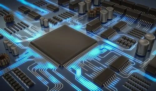
Professional PCB manufacturing and assembly
Building 6, Zone 3, Yuekang Road,Bao'an District, Shenzhen, China
+86-13410863085Mon.-Sat.08:00-20:00

What are the benefits of analyzing boundary scan testing for PCB assembly?
When conducting PCB assembly test, it is usually regarded as an increased expenditure, rather than as an essential quality control measure, thus bringing great value to the final product. Even before studying the benefits of boundary scanning for PCB assembly testing, it is important to answer the question why people need to conduct PCB assembly testing first.
The answer to why testing is only the fact that this is the only way to ensure product quality. Therefore, it is better to regard it as a mechanism rather than an expenditure, which can avoid the company's costly mistakes in the future, which in turn will waste time, money and important company reputation. On the other hand, insufficient testing may lead to defective products reaching the end users, which may require replacement or recall, and may cause irreparable damage to the company's reputation, or even costly litigation.
It is essential to determine the appropriate amount of testing in order to ensure that product quality soars without testing costs. Of course, the amount of testing may vary from industry to industry. For example, mission critical operations will require extensive testing, while certain product defects are acceptable in certain industries.
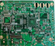
Main contents of PCB assembly test
When we talk about the testing process, we need to conduct a comprehensive evaluation of three aspects. These include:
Structural devices
Structural connection
Functional connection
In order to test all three aspects, several test methods can be used:
Visual test
Automated optical inspection
X-ray inspection
Online test
JTAG boundary scan
Customized test software
It is essential that the test method used must cover the entire range of potential failure categories so that defect coverage scores can be determined. This largely involves a method commonly known as PCOLA/SOQ/FAM. Essentially, this is an end-to-end approach that covers the entire test scope, as shown below:
PCOLA
This part involves structural equipment and relies on visual testing. It is an acronym for presence, correctness, orientation, activity and alignment, and it carefully studies all these aspects to ensure that no defects are found.PCB processing, PCB design. The PCB assembly factory explained and analyzed the advantages of boundary scan test for PCB assembly? PCB assembly test.
SOQ
Unlike PCOLA, which relies on visual testing, this part depends on electrical testing methods. SOQ is the acronym of Shorts, Opens and Quality, and the connectivity test is carried out so that there is no problem with the electrical connection.
FAM
This aspect involves functional testing as well as functional, full speed and measurement checks. Therefore, these tests can ensure that the system operates according to the set benchmark.
Correlation between Boundary Scan and PCB Assembly Test
In order to save costs, it is necessary to determine which test methods need to be used to cover the entire scope. This is where boundary scanning becomes extremely important. The main advantages of boundary scanning are as follows:
This is very relevant when physical access is restricted
It covers a large part of PCOLA/SOQ/FAM spectrum, so it has a wide coverage
Because of its wide coverage, it eliminates the need for other structural testing methods, thereby saving costs.
For example, compared with ICT and other methods, it is much less cost intensive, while ICT and other methods require test fixture and equipment maintenance. Although JTAG boundary scan does require costs such as equipment, training and labor costs, it is still the best choice in terms of overall cost.
It provides low test time, which is a huge advantage in today's fierce competition because it can shorten the time to market.
Needless to say, it is accompanied by an increase in product output, which is exactly the purpose of the test.
All aspects must be considered when selecting the test method. These include the coverage provided, costs incurred, etc. The boundary scan stands out from all these parameters. It provides versatility and affordability. Not surprisingly, it is one of the most popular methods in PCB assembly testing.The PCB processing factory explained and analyzed the advantages of boundary scan test for PCB assembly? PCB assembly test.


Just upload Gerber files, BOM files and design files, and the KINGFORD team will provide a complete quotation within 24h.