
Professional PCB manufacturing and assembly
Building 6, Zone 3, Yuekang Road,Bao'an District, Shenzhen, China
+86-13410863085Mon.-Sat.08:00-20:00

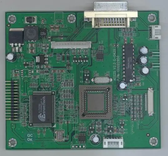
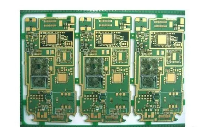
We all know the whole word of assembly panel, especially proofing, from friends who have been exposed to circuit boards. What does assembly panel mean? What should we pay attention to in the process of splicing? Now let's summarize the precautions for circuit board assembly.
The outer frame (clamping edge) of the PCB panel shall adopt a closed loop design to ensure that the PCB panel will not deform after being fixed on the fixture;
2. PCB panel width ≤ 260mm (SIEMENS line) or ≤ 300mm (FUJI line); If automatic dispensing is required, PCB panel width × Length ≤ 125 mm × 180 mm;
3. PCB panel shape should be as close to square as possible, and 2 is recommended × 2、3 × 3. ...... Panel; But do not make up the yin and yang plates;
4. The center distance between small plates shall be controlled between 75 mm and 145 mm;
5. When setting the datum locating point, a non blocking area 1.5 mm larger than the locating point is usually reserved around the locating point;
6. There shall be no large components or protruding PCB components near the connection point between the outer frame of the panel and the internal small board, or between the small board and the small board, and a space of more than 0.5mm shall be reserved at the edge of the PCB components and PCB board to ensure the normal operation of the cutting tool;
7. Make four positioning holes at the four corners of the outer frame of the panel, with the hole diameter of 4mm ± 0.01mm; The strength of the hole shall be moderate to ensure that it will not break during the process of upper and lower plates; The hole diameter and position accuracy shall be high, and the hole wall shall be smooth without burrs;
8. Each small board in the PCB assembly must have at least three positioning holes, 3 ≤ hole diameter ≤ 6 mm, and no wiring or patch is allowed within 1mm of the edge positioning hole;
9. In principle, QFP with spacing less than 0.65mm shall be set at its diagonal position for the reference mark used for PCB whole board positioning and fine pitch device positioning; The positioning datum symbols used for the sub boards of the assembled PCB shall be used in pairs and arranged at the opposite corners of the positioning elements;
10. Large PCB components shall be provided with positioning posts or holes, especially I/O interfaces, microphones, battery interfaces, microswitches, headphone interfaces, motors, etc;


Just upload Gerber files, BOM files and design files, and the KINGFORD team will provide a complete quotation within 24h.