
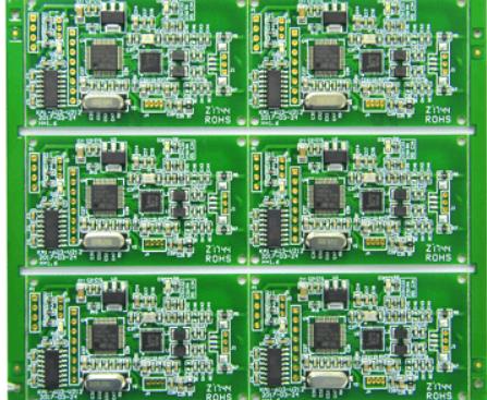
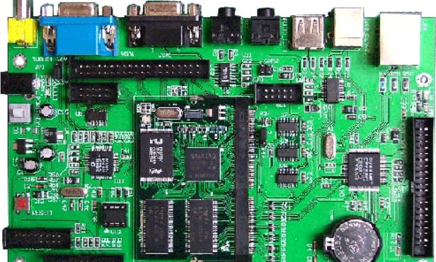
Professional PCB manufacturing and assembly
Building 6, Zone 3, Yuekang Road,Bao'an District, Shenzhen, China
+86-13410863085Mon.-Sat.08:00-20:00

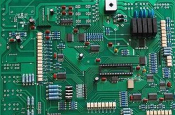
Popular SMT chip SMT and chip professional welding
SMT: Abbreviation of English surface mounting technology, Chinese means surface mounting (mounting) technology, a technology for welding electronic parts to the surface of circuit boards As a new generation of electronic assembly technology, SMT products have the advantages of compact structure, small size, vibration resistance and high production efficiency Surface mount technology occupies a leading position in the circuit board assembly process Main equipment of SMT assembly line: printing machine, mounting machine, reflow soldering, etc
Why is smt chip processing technology so popular? Advantages of SMT chip processing:
1. Small size and high assembly density of electronic products
The volume of SMT chip module is only about 10% of the traditional package module, and the weight is only 10% of the traditional chip module.
2. High reliability and strong anti vibration capability
SMT chip processing adopts chip components with high reliability, small size, light weight, strong anti vibration ability, automatic production, high installation reliability and low solder joint defect rate.
Because the chip modules are firmly installed, the devices are usually lead-free or short leads, which reduces the impact of parasitic inductance and capacitance, improves the high-frequency characteristics of the circuit, and reduces electromagnetic and radio frequency interference.
4. Improve production efficiency and realize automatic production
Automatic placement machine (Yamaha automatic placement machine ysm-10/ysm-20) uses vacuum nozzle to suction and release components. The shape of the vacuum nozzle is smaller than that of the components, thus increasing the installation density.
5. Reduce costs and expenses
SMT patch processing technology can save data, energy, equipment, labor, time, etc, Costs can be reduced by 30% and 50%!
It is precisely because of the complexity of SMT wafer processing process flow that there are many SMT wafer processing plants specializing in SMT wafer processing.
Professional welding method of SMT chip
1. First, clamp the wafer with tweezers and align the pads:
In order to meet the needs of e-lovers, the Fortune Creation Platform provides a free e-learning platform, mainly to let more e-lovers get a quick start. Our platform has many years of senior engineers, R&D engineers, FAE fault analysis engineers, powerRD, HardwareRD, SoftwareRD, senior automation RD, technical directors, etc., to integrate social status and plant development
2. Then press the chip with your thumb:
Before proceeding to the next step, please make sure that the wafer is aligned with the pad, otherwise it will be more troublesome to find that the wafer is not aligned after the next step. Then take a small piece of rosin with tweezers and place it next to the pin of D12 chip. Note that rosin is used here instead of thicker flux (this flux cannot hold wafers):
The next step is to melt the rosin with a soldering iron. Rosin has two functions here: one is to fix the chip on the PCB, and the other is to help with welding, ha ha. When melting rosin, it is necessary to dissolve as much rosin as possible and distribute it evenly on a row of mats.
5. Then fix the pin on the other side of D12 with rosin After this step, D12 will firmly fix the PCB. Remember, before checking whether the chip is correctly aligned with the bonding pad, or wait for rosin to be coated on both sides It's hard to take it after finishing
If you accidentally put too much at one time, there is no solution. If it is just a little more, you can drag left and right as shown in the video tutorial, so that the extra tin is evenly distributed to each pad to solve the problem; If more is needed, other methods should be used. It is recommended to use suction cups to suck out excess solder
7. Melt the solder with a soldering iron, and then drag the soldering iron to the right along the contact point between the pin and the pad until it reaches the rightmost pin:
For example, all pins on one side of D12 can be welded, and the other side can be welded in the same way. At the same time, you can also refer to the following videos for practice.
SMT: Abbreviation of English surface mounting technology, Chinese means surface mounting (mounting) technology, a technology for welding electronic parts to the surface of circuit boards As a new generation of electronic assembly technology, SMT products have the advantages of compact structure, small size, vibration resistance and high production efficiency Surface mount technology occupies a leading position in the circuit board assembly process Main equipment of SMT assembly line: printing machine, mounting machine, reflow soldering, etc
Why is smt chip processing technology so popular? Advantages of SMT chip processing:
1. Small size and high assembly density of electronic products
The volume of SMT chip module is only about 10% of the traditional package module, and the weight is only 10% of the traditional chip module.
2. High reliability and strong anti vibration capability
SMT chip processing adopts chip components with high reliability, small size, light weight, strong anti vibration ability, automatic production, high installation reliability and low solder joint defect rate.

Because the chip modules are firmly installed, the devices are usually lead-free or short leads, which reduces the impact of parasitic inductance and capacitance, improves the high-frequency characteristics of the circuit, and reduces electromagnetic and radio frequency interference.
4. Improve production efficiency and realize automatic production
Automatic placement machine (Yamaha automatic placement machine ysm-10/ysm-20) uses vacuum nozzle to suction and release components. The shape of the vacuum nozzle is smaller than that of the components, thus increasing the installation density.
5. Reduce costs and expenses
SMT patch processing technology can save data, energy, equipment, labor, time, etc, Costs can be reduced by 30% and 50%!
It is precisely because of the complexity of SMT wafer processing process flow that there are many SMT wafer processing plants specializing in SMT wafer processing.
Professional welding method of SMT chip
1. First, clamp the wafer with tweezers and align the pads:
In order to meet the needs of e-lovers, the Fortune Creation Platform provides a free e-learning platform, mainly to let more e-lovers get a quick start. Our platform has many years of senior engineers, R&D engineers, FAE fault analysis engineers, powerRD, HardwareRD, SoftwareRD, senior automation RD, technical directors, etc., to integrate social status and plant development
2. Then press the chip with your thumb:
Before proceeding to the next step, please make sure that the wafer is aligned with the pad, otherwise it will be more troublesome to find that the wafer is not aligned after the next step. Then take a small piece of rosin with tweezers and place it next to the pin of D12 chip. Note that rosin is used here instead of thicker flux (this flux cannot hold wafers):
The next step is to melt the rosin with a soldering iron. Rosin has two functions here: one is to fix the chip on the PCB, and the other is to help with welding, ha ha. When melting rosin, it is necessary to dissolve as much rosin as possible and distribute it evenly on a row of mats.
5. Then fix the pin on the other side of D12 with rosin After this step, D12 will firmly fix the PCB. Remember, before checking whether the chip is correctly aligned with the bonding pad, or wait for rosin to be coated on both sides It's hard to take it after finishing
If you accidentally put too much at one time, there is no solution. If it is just a little more, you can drag left and right as shown in the video tutorial, so that the extra tin is evenly distributed to each pad to solve the problem; If more is needed, other methods should be used. It is recommended to use suction cups to suck out excess solder
7. Melt the solder with a soldering iron, and then drag the soldering iron to the right along the contact point between the pin and the pad until it reaches the rightmost pin:
For example, all pins on one side of D12 can be welded, and the other side can be welded in the same way. At the same time, you can also refer to the following videos for practice.


Just upload Gerber files, BOM files and design files, and the KINGFORD team will provide a complete quotation within 24h.