
Professional PCB manufacturing and assembly
Building 6, Zone 3, Yuekang Road,Bao'an District, Shenzhen, China
+86-13410863085Mon.-Sat.08:00-20:00

Cause Analysis and Prevention of PCBA Assembly Explosion -- Cause Analysis of Plate Explosion
1 What is a bursting plate
Burst board is a common name for delamination or blistering of printed boards.
Delamination is the separation between layers in the substrate, between the substrate and the conductive copper foil, or in any other layer of the printed board.
Foaming is a delamination characterized by local expansion and separation between any layers of the laminated substrate or between the substrate and the conductive copper foil or protective coating. Bubbling is also a form of stratification.
2. Analysis of plate bursting causes
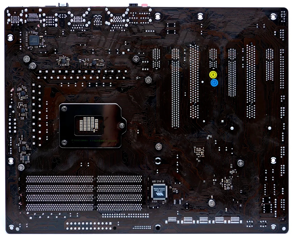
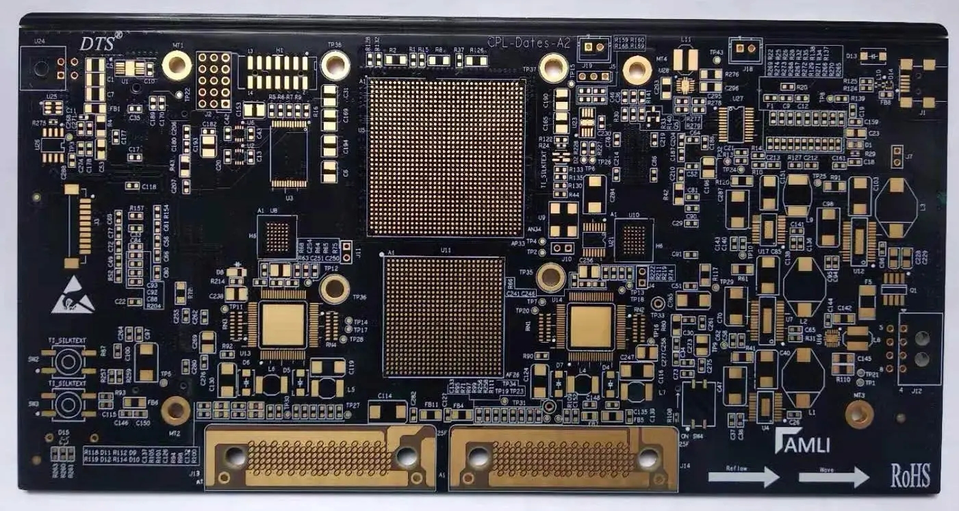
The customer's products are used in the frequency converter of industrial control. The design requirement is the PCB with CTI value. This 4-layer PCB has special requirements in the production and application process. Due to the particularity of the material of the copper clad laminate with CTI>600, it cannot be directly pressed with the inner line. This type of panel must be pressed with different types of interlayer insulating semi solidified sheet materials in order to meet the process requirements of CTI and lamination bonding force at the same time.
As two kinds of semi curing sheet insulating materials are used for pressing, the two materials have different resin types. Compared with the single insulating material of conventional 4-layer board, the bonding force of the fusion interface of the insulating materials in the second layer is relatively small. When the printed circuit board absorbs moisture to a certain extent under natural conditions, and when the wave soldering or manual plug-in soldering is performed, the PCB rises from the normal temperature to above 240 degrees Celsius, the moisture absorbed in the board is instantly heated, expanded and vaporized, and huge pressure is generated inside. When the pressure is greater than the bonding force of the insulating layer in 2, the board will explode.
Generally, plate bursting is caused by congenital defects in materials or processes. As for the material, it is copper clad plate or PCB, and the process includes the production process of copper clad plate and PCBA board, the production process of PCB, and the PCBA assembly process.
(1) Moisture absorption during PCB manufacturing
The raw materials of PCB have good affinity for water and are easy to absorb moisture. The following shows that the existence of water vapor is the primary cause of PCB bursting through the existence form of water in PCB, the way of water vapor diffusion, and the pressure change of water vapor pressure with temperature.
The water in PCB mainly exists in the resin molecules and the physical structure defects in PCB. The water absorption rate and equilibrium water absorption capacity of epoxy resin are mainly determined by the free volume and the concentration of polar groups. The larger the free volume is, the faster the initial water absorption rate will be. The polar group has affinity for water, which is also the main reason why epoxy resin has high moisture absorption capacity. The larger the content of polar group is, the greater the balanced water absorption capacity will be. On the one hand, when PCB reflow soldering or wave soldering, with the increase of temperature, water in its own volume and water with limit groups forming hydrogen bonds can obtain enough energy to do diffusion movement in the resin. The water diffuses outward and gathers at the defects of the physical mechanism, whose molar volume increases. On the other hand, with the increase of welding temperature, the saturated vapor pressure of water also increases.
According to the data, with the rise of temperature, the saturated vapor pressure also rises sharply, reaching 400P/kPa at 250 ℃. When the adhesion between the layers of the material is lower than the saturated vapor pressure generated by water vapor, the material will be delaminated or bubbled. Therefore, moisture absorption before welding is the main reason for PCB bursting.
(2) Moisture absorption during PCB storage
PCBs with CTI>600 should be listed as moisture sensitive devices. The presence of moisture in PCBs has an extremely important impact on their assembly and performance. When PCBs with high CTI values are stored without moisture or poor moisture resistance, they agree to cause moisture absorption. Obviously, under static storage conditions, with the promotion of time, the moisture content of PCBs will gradually increase, and the difference between the water absorption of vacuum packaging and the water absorption of vacuum packaging with the temporary storage time.
(3) Long term moisture absorption during PCBA production
During the production process, PCBA with CTI>600 may also absorb moisture if it is exposed for a long time due to materials or other factors. If welding is carried out after moisture absorption, there is also a risk of plate bursting.
(4) Poor welding curve of PCBA lead-free process
For the lead-free process of PCBA, Sn53/Pb87 solder has been replaced by SnAg Cu lead-free solder. Its melting point has risen from 183 ℃ to more than 217 ℃. The temperature of reflow welding and wave soldering has risen from 230 ℃ to 235 ℃ to 250 ℃ to 255 ℃. The peak temperature may be higher. In the process of welding, if the welding time is long, the sharp increase of welding heat will magnify the factors due to poor PCB fabrication, and the possibility of plate bursting will increase.


Just upload Gerber files, BOM files and design files, and the KINGFORD team will provide a complete quotation within 24h.