
Professional PCB manufacturing and assembly
Building 6, Zone 3, Yuekang Road,Bao'an District, Shenzhen, China
+86-13410863085Mon.-Sat.08:00-20:00


Explanation of tin bead in PCBA processing
What are the requirements of acceptable standards for tin beads in PCBA processing
The so-called PCBA processing refers to the entire production process of PCB boards through SMT chip processing, DIP plug-in processing, assembly and testing.
The basic core processing technology of PCBA processing (Printed Circuit Board Assembly) is to load the blank PCB through SMT, and then through DIP plug-in. SMT and DIP are both ways to integrate parts on a PCB. The main difference is that SMT does not need to drill holes on a PCB. In DIP, the PIN pin of the part needs to be inserted into the drilled hole.
SMT (Surface Mounted Technology) surface mounting technology mainly uses the mounting machine to mount some micro and small parts onto PCB boards. Its production process includes PCB board positioning, printing solder paste, mounting by the mounting machine, soldering back to the furnace and manufacturing inspection. With the development of science and technology, SMT can also mount some large-sized parts, for example, some large-sized mechanism parts can be mounted on the motherboard.
DIP is "plug-in", that is, insert parts on PCB board. Because the part size is large and it is not suitable for mounting or the manufacturer cannot use SMT technology in production process, the plug-in form is used to integrate parts. At present, there are two ways to realize the manual plug-in and robot plug-in in the industry, and the main production processes are: adhesive backing (to prevent tin plating to the wrong place), plug-in, inspection, wave soldering, plate brushing (to remove the stains left in the furnace process) and manufacturing inspection.
SMT and DIP are important processes in PCBA processing.
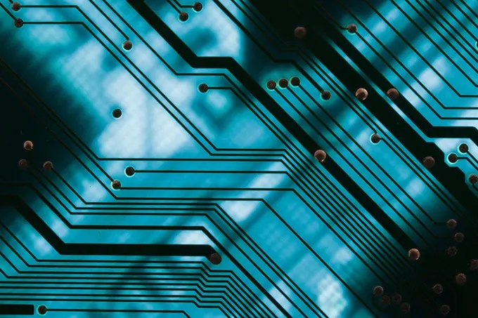
In the processing and production of the smt processing plant, there will be a bad phenomenon, that is, the tin bead phenomenon, which is one of the main defects in the smt chip technology and often troubles the staff of the electronic processing plant. It is inevitable that some tin beads remain on the surface of the board during PCBA processing, so it is acceptable for tin beads that meet the standards.
In the processing and production of the smt processing plant, there will be a bad phenomenon, that is, the tin bead phenomenon, which is one of the main defects in the smt chip technology and often troubles the staff of the electronic processing plant. It is inevitable that some tin beads remain on the surface of the board during PCBA processing, so it is acceptable for tin beads that meet the standards.
What are the requirements of acceptable standards for tin beads in PCBA processing
Acceptable standard of tin bead:
1. Tin bead diameter shall not exceed 0.13mm
2. The number of tin beads with a diameter of 0.05mm-0.13mm within the range of 600mm2 shall not exceed 5 (single side)
3. No requirement for the number of tin beads with a diameter below 0.05
4. All tin beads on the PCBA board must be wrapped by the flux and cannot be moved (if the flux is wrapped to more than 1/2 of the height of the tin bead, it is regarded as wrapped)
5. Tin bead does not reduce the electrical clearance of different network conductors to less than 0.13mm
The appearance inspection standard of smt chip technology products is the most basic standard for electronic product acceptance. According to different products and customers' requirements, the requirements for the acceptability of tin beads will vary. Generally, the standard is determined on the basis of national standards and customers' requirements.
Conformation coating of PCBA components
Oct 28,2022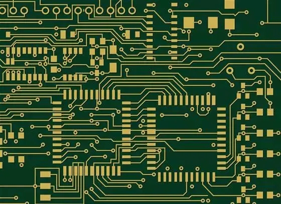


Just upload Gerber files, BOM files and design files, and the KINGFORD team will provide a complete quotation within 24h.