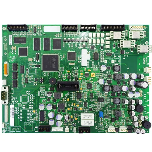
Medical PCB Board Blood Pressure Monitor PCBA Assembly Supplier
PCB Assembly Name:Medical PCB Board Blood Pressure Monitor PCBA Assembly Supplier
Surface Finishing:HASL, Enig, OSP, Immersion Au, AG, Sn
MOQ:1 PCS
Layer:1-18 Layer
Copper Thickness:0.5oz-6oz
Board Thickness:0.2mm-4mm
Min.Hole Size:0.1mm (4 Mil)
Min.Line Spacing:0.1mm (4 Mil)
PCBA QC:X-ray, Aoi Test, Function Test(100% Test)
Specialised:Consumer, LED, Medical, Industrial, Control Board
Delivery:PCB, 7-10 Days;PCBA, 2-3weeks
Service:PCBA/PCB Assembly/PCB Circuit Board
Other Service:PCB/PCB Layout and Design, Engineering Support
Transport Package:Vacuum Packing/Blister/Plastic /Cartoon
Specification:CE, RohS, UL, SGS, ISO9001: 2015, ISO 14001
Trademark:One Stop Manufacturer PCBA PCB Assembly
Origin:Shenzhen, Guangdong
Production Capacity:5, 000, 000PCS /Month
Cleanliness of Electronic PCB Assemblies Leads to Medical Device Reliability
Overcoming the Potential for Failures
Component manufacturers are continually developing new and smaller packages for components that are mere fractions of a millimeter and have board to component clearances of less than a mil. Pick and place machines have new accessories that allow placement of these almost invisible parts. Components are placed extremely close together. How do you effectively clean under something so small?
No lead solder is a relatively recent legislated fact of life that necessitated new solder, new fluxes, higher temperatures, and new solder processing equipment. Many new approaches, alloys, chemicals, and soldering processes have been developed to address these issues. Tin whisker problems also increased dramatically. Time-delayed effects, however, often will not show up until a product is out the door and has been in service for even a year or two. The pace of product development covers up some of these time-delayed issues when products are routinely discarded for newer models. For products such as mobile phones, problems don’t often show up because comparatively few people are using a mobile phone that is more than 2-3 years old. Few will spend money for repair when an upgraded feature-rich model is available at a subsidized price. For medical devices, however, the potential for failure is very real and the effects of failure can be devastating.
Design Decisions Impact Other Process Steps
The single place where it all comes together and where the supporting elements have to operate properly is the manufacturing floor, but often component manufacturers, board designers, and the device manufacturer are operating independently of one another and this communication void exacerbates the problem. Research shows that many failures are a result of printed circuit boards (PCBs) that are not clean enough of contaminants from the manufacturing process. There are design issues that are enabled by the advanced CAD design systems utilized for PCB design.
Sometimes a designer will utilize features such as ultra-close copper pour or fill that puts a ground a few mils from a power bus all over the board. The opportunity for shorts with catastrophic consequences just increased several fold. Many designers have little exposure to the production issues of PCB fabrication or board assembly. It’s important for a board designer to really understand how flux from the hand soldering process of a connector can flow to the microvia that was placed right next to a connector pad. Many decisions one makes in implementing a design will impact the other process steps.
Standards Need to Be Raised for High Reliability
IPC, the global trade association serving the printed board and electronics assembly industries, their customers, and suppliers, has a task group devoted to addressing all topics connected with determining the cleanliness levels of unpopulated (bare) printed circuit boards and has established a base standard for cleanliness. The IPC-TM-650 standard sets an acceptable range of 10-2 micrograms/in2 for military applications (65-2 micrograms/in2 for general applications) of sodium chloride (NaCl). Is this standard enough to prevent failures and can present cleaning methods truly clean the boards that are being produced today?
There are a number of myths circulating in the industry:
1. All bare boards coming from the fab house are clean.
2. All components are delivered clean with no contamination issues.
3. Flux will never present any problems and can just be poured onto the board without worrying about heating or the absence of heat and everything will work out okay.
This is not the reality in manufacturing today, but the assumption of these concepts presents major issues for the manufacturer. A board with hidden residual flux contamination may pass QC and operate properly. After arriving in its operating environment there may be high humidity and temperature swings that generate condensation that causes residual flux problems to literally begin to grow and eventually cause leakage paths that ultimately cause failures. The high impedance circuits of today’s micropower electronics are even easier to disrupt with stray voltage sources.
Simple Washing Is Not Enough
Washing a printed circuit board after the soldering process typically produces a board that sparkles and looks ready for the next step of its journey to the end user. The areas that are not visible contain the details that spoil this sparkling clean picture. It's not enough to put the boards through a wash cycle. It takes a special combination of chemicals, temperature, wash cycles, and timing to get the boards really clean.
“The cleanliness of a printed board can directly impact the effectiveness or quality of an assembled printed board,” said John Perry, IPC technical project manager and staff liaison to IPC’s Bare Board Cleanliness Assessment Task Group. “Residues increase the risk of field failures or can electrically impede a printed board’s function, so having acceptance criteria for various levels of testing as well as direction on how many samples should be tested is extremely important.”
Digicom Electronics utilized significant resources to research these issues. In many instances, it was found that a combination of comparatively minor points, when combined, pointed to processes that simply did not work as well in today’s manufacturing environment, though their performance in times past was adequate. Minor changes in component packaging design, materials, CAD/CAM software, board fabrication, and chemistry combined to slowly change the robustness of the manufacturing process. Even the best intentions have often unwittingly created the potential for defects to occur in ways not previously possible. It was only through a comprehensive evaluation of all materials and steps in the manufacturing process that root causes of potential problems were discovered. Armed with a clear picture of potential problem areas, much effort was expended to find solutions to each problem.
New equipment and supporting subsystems were ordered and installed. Test and evaluation procedures were developed and implemented to verify the effectiveness of each process. All boards were routinely run through the system both prior to and after the assembly process to ensure that the soldering process was not compromised by any contaminates from the board fabrication process and that the boards were completely clean of any remaining chemicals from soldering.
The cleaning process is completely green. De-ionized water from polishing tanks is used and recycled. Filters catch the solids while powerful blowers ensure that harsh chemicals don’t migrate passed the holding tank. Clear windows on the equipment enable the operator to monitor the entire process. A refractometer checks the stability of the mix in the tank to see that it’s not compromised. The discharged liquid is completely environmentally friendly.
Processes were then thoroughly tested, evaluated for effectiveness, and ultimately validated as a stable process. Independent tests showed that boards that went through this cleaning process tested 75% cleaner than the 10-2 micrograms/in2 specified by IPC as its highest level of clean. In addition, a lab analysis for ion contamination found zero levels of sodium chloride ion contamination on the assembled boards.
Kingford supports Medical PCB Board Blood Pressure Monitor Assembly Supplier business, we are a professional PCBA one-stop assembly factory, welcome to place an order
")
PCB Assembly Name:Medical PCB Board Blood Pressure Monitor PCBA Assembly Supplier
Surface Finishing:HASL, Enig, OSP, Immersion Au, AG, Sn
MOQ:1 PCS
Layer:1-18 Layer
Copper Thickness:0.5oz-6oz
Board Thickness:0.2mm-4mm
Min.Hole Size:0.1mm (4 Mil)
Min.Line Spacing:0.1mm (4 Mil)
PCBA QC:X-ray, Aoi Test, Function Test(100% Test)
Specialised:Consumer, LED, Medical, Industrial, Control Board
Delivery:PCB, 7-10 Days;PCBA, 2-3weeks
Service:PCBA/PCB Assembly/PCB Circuit Board
Other Service:PCB/PCB Layout and Design, Engineering Support
Transport Package:Vacuum Packing/Blister/Plastic /Cartoon
Specification:CE, RohS, UL, SGS, ISO9001: 2015, ISO 14001
Trademark:One Stop Manufacturer PCBA PCB Assembly
Origin:Shenzhen, Guangdong
Production Capacity:5, 000, 000PCS /Month