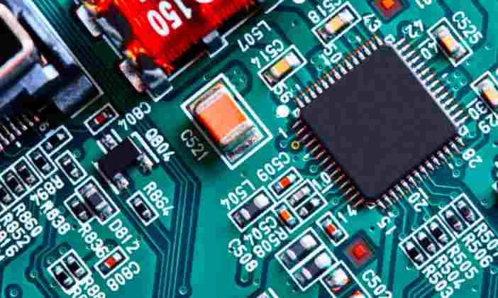
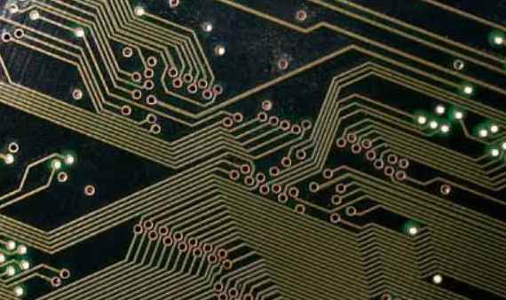
How to prevent PCB board from bending and warping in back welding furnace
In PCB board backwelding furnace prone to plate bending and plate warping, we all know, so how to pr...

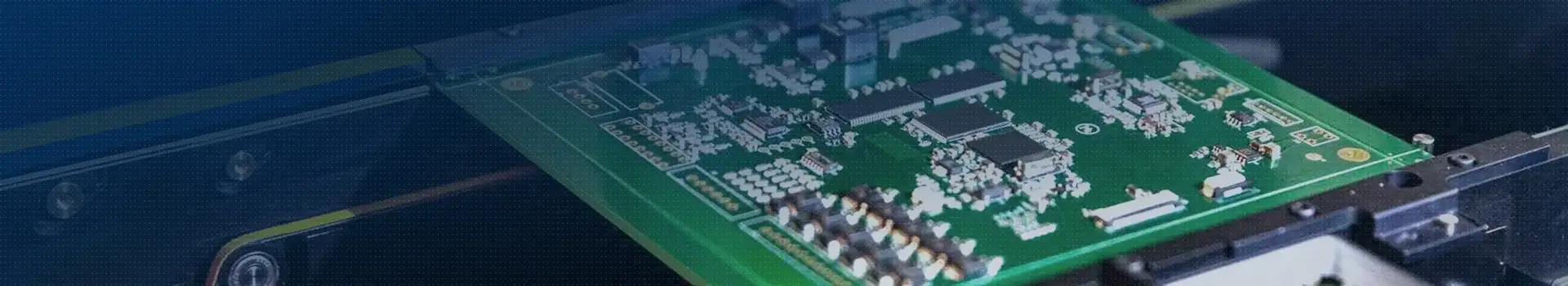
In PCB board backwelding furnace prone to plate bending and plate warping, we all know, so how to pr...
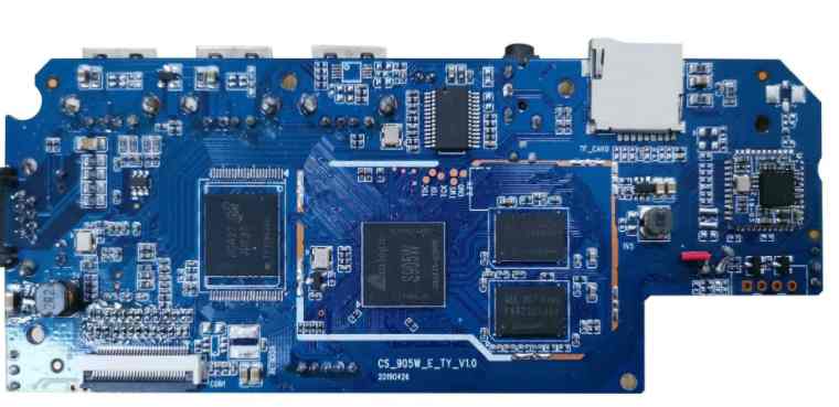
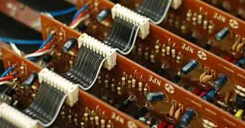
PCBA OEM has three main functions: 1. Assembly chip, 2. Processing, 3. test
The PCB is then placed into the developer to remove unwanted solder masks so that the specified copp...
How to improve customer satisfaction of PCBA assembly plant: first, PCBA assembly plant positioning,...
Compared with the circuit material without microsphere packing, the RO4730G3 circuit material with h...
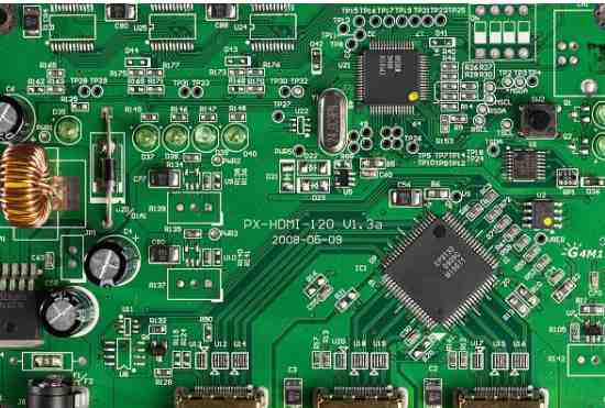
Specifications for PCB storage and inspection in SMT factories: 1. PCB inspection standards and insp...
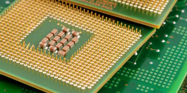
Printed circuit board A flat plate made of non-conductive material, usually with pre-drilled holes d...
The finger contains a number of exposed copper pads that are actually part of the PCB wiring. Usuall...
By analyzing the causes of PCB size increase and contraction, we can find out the available monitori...
For high - level circuit board processing technology research literature, the industry is relatively...
According to the laminated structure of the high-rise board and the materials used, study the approp...
Due to the number of high-rise board layers, the customer design end of PCB layer alignment requirem...
