
Professional PCB manufacturing and assembly
Building 6, Zone 3, Yuekang Road,Bao'an District, Shenzhen, China
+86-13410863085Mon.-Sat.08:00-20:00

Solve EMC PCB design from layering, layout and routing
Adding this option to the interior belongs to component and circular design.<one href="one _href_0" t-rget="_self">Good PCB design is a very important factor in the electromagnetic compatibility of the interior The key to the PCB design is to reduce the reflow area and allow the reflow path to flow in the design direction The common problems come back from... starting the crack in the reference plane, converting the reference plane layer, and the signal flow through the connector Jumping capacitors or decoupling capacitors may solve some problems, but the overall impedance of capacitors, vias, pads, and traces must be considered This speech will introduce EMC's PCB design technology from three aspects: PCB layering strategy, layout skills and wiring rules
1. PCB layering strategy
The thickness, through-hole process and number of layers of circuit board are not the key to solve the problem in circuit board design. The excellent layered stacking is to ensure the bypass and decoupling of the power bus, so that the transient voltage on the power plane or the ground plane is not affected. The key to mask signals and power electromagnetic fields. From the point of view of signal routing, a good layering strategy should be to place all signal traces on one or more layers next to the power or ground plane. For power supply, a good layering strategy should be that the power layer is adjacent to the ground layer, and the distance between the power layer and the ground layer should be as small as possible. This is what we call "layering" strategy. Now we will specifically discuss a good PCB layering strategy.
1) The projection plane of the wiring layer shall be within the area of its return plane layer. If the wiring layer is not within the projection area of the return plane layer, there will be signal lines outside the projection area during wiring, which will lead to the "edge radiation" problem, and also lead to new signal loop area, resulting in new differential mode radiation.
2.) Try to avoid setting adjacent wiring layers. Since the parallel signal track on adjacent wiring layers will cause signal crosstalk, if it is impossible to avoid adjacent wiring layers, the layer spacing between two wiring layers should be added appropriately, and the layer spacing between wiring layers and their signal loops should be reduced.
3.) The adjacent plane layers shall avoid overlapping of their projection planes. Because when the projections overlap, the coupling capacitance between layers will cause the noise between layers to be coupled.
2. Multilayer board design:
When the clock frequency exceeds 5. MHz or the signal rise time is less than 5 nanoseconds, in order to control the signal loop area well, it is usually necessary to use a multilayer board design. When designing multilayer boards, the following principles should be noted:
1) The key wiring layer (the layer where the clock line, bus bar, interface signal line, RF line, reset signal line, chip selection signal line and various control signal lines are located) should be close to the entire ground plane, preferably between two ground planes. The key signal lines are usually strong radiation or extremely sensitive signal lines, and the wiring close to the ground can reduce the area of the signal loop, reduce its radiation intensity or improve the anti-interference ability.
2) The power panel shall be retracted relative to its adjacent ground plane (the recommended value is 5H~20H). Relative to returning to the ground plane to shrink the power plane, it can effectively suppress the "edge radiation" problem. In addition, the main working power plane of the circuit board (widely used) should be close to its ground plane to effectively reduce the loop area of the power current.
3) Check whether there is no 50MHz signal line on the top and bottom layers of the circuit board. If so, high frequency signals are routed between the two plane layers to suppress their radiation to space.
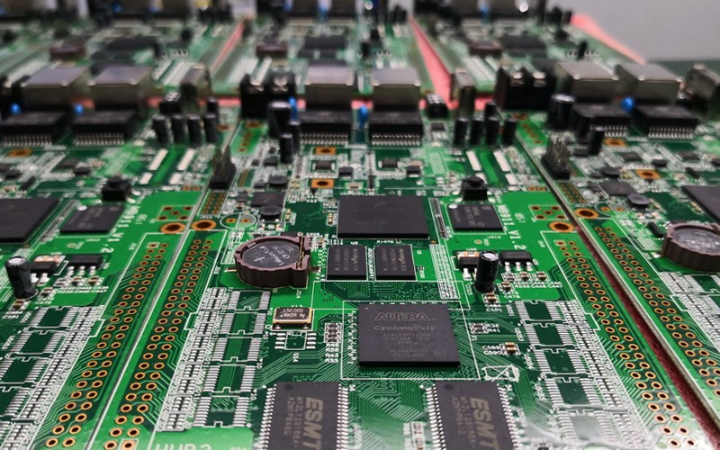
Circuit board
3. Single layer and double layer plate design:
For the design of single layer board and double layer board, the design of key signal lines and power lines shall be mainly focused. There must be grounding wire near the power line and parallel line to reduce the area of the power current loop. The "leading ground wire" shall be placed on both sides of the key signal line of the single-layer board. The projection plane of the key signal lines of the double-layer board shall have a large area of ground, or the design of "guide ground wire" shall be the same as that of the single-layer board. On the one hand, the "protective area" on both sides of the key signal line can reduce the area of the signal loop, and on the other hand, it can prevent the crosstalk between the signal line and other signal lines.
4... PCB Layout Skills
When designing the layout of the printed circuit board, the design principle of placing it in a straight line along the signal flow direction shall be fully observed, and the front and back loops shall be avoided as far as possible. This can avoid the direct coupling of the signal and will affect the signal quality. In addition, in order to prevent mutual interference and coupling between circuits and electronic components, the layout of circuits and components shall follow the following principles:
1) If the "clean floor" is designed on the interface panel, the filtering and isolation devices should be placed on the isolation belt between the "clean floor" and the working floor. This can prevent the filtering or isolation devices from coupling with each other through the plane layer, thus weakening the effect. In addition, "clean" means that no other devices should be placed except the filtering and protective devices.
2) When multiple modular circuits are placed on the same printed circuit board, digital circuit and analog circuit, high-speed and low-speed circuits shall be separated to avoid mutual interference between digital circuit, analog circuit, high-speed circuit and low-speed circuit. In addition, when high-speed, medium speed and low-speed circuits exist on the circuit board at the same time, in order to prevent high-frequency circuit noise from radiating outward through the interface.
3. The filter circuit of the power input port of the circuit board shall be close to the interface to avoid re coupling of the filter circuit.
4. The filtering, protection and isolation devices of the interface circuit are placed close to the interface, which can effectively achieve the effects of protection, filtering and isolation. If there are filtering and protection circuits at the interface, the principle of protection before filtering shall be followed. Since the protection circuit is used for external overvoltage and overcurrent suppression, if the protection circuit is placed behind the filter circuit, the filter circuit will be damaged due to overvoltage and overcurrent. In addition, due to the mutual coupling between the input and output lines of the circuit, the filtering, isolation or protection effects will be weakened. During layout, ensure that input and output lines of filter circuit (filter), isolation and protection circuit are not coupled with each other.
5) Sensitive circuits or devices (such as reset circuits) shall be at least 1000 mils away from each edge of the board, especially the edge of the board interface side.
6) Energy storage and high-frequency filter capacitors shall be placed near unit circuits or equipment with large current changes (such as input and output terminals of power modules, fans and relays) to reduce the loop area of large current loops.
7) The filter elements should be placed side by side to prevent the filter circuit from being disturbed again.
8) Crystals, crystal oscillators, relays, switching power supplies and other strong radiation equipment shall be at least 1000mm away from the single board interface connector. In this way, the interference can be directly radiated to the outside, or the current can be coupled to the output cable to radiate outward.
5. (Printed Circuit Board) Board Wiring Rules
In the inside, a dd, it is i on... to comp, nt, select i on... and circular design,<strong>good printed circuit board (printed circuit board) layout is a l, so a very imp or t, nt, f, c to r electromagnetic comp in the inside is y on ibil S In the inside, the printed circuit board (CE) is a parent comp in the inside, and the parent comp in the... belongs to this system. ENH - NC in the inside, G electromagnetic comp in the ibil, Y in the inside, and this printed circuit board route will not be forced to implement an additional cost in the..., F in the inside, and 1 product Any should keep "e" in "m" in "d" which po or PCB layout can cause "m" or "e" EMC problems, "s" in "e" in "m", and "es" in "c", even if "dd" in "g filter" s "and" comp "in" nts "are not the same as" lve "m There is a whole plate of re wire This ref or e, develop in g Good PCB r comes out in g h - b Its in this is g in n in g is this method to save m in The following will introduce some general rules that pertain to PCB wiring and the design str belongs to power line, ground wire s and signal line s Acc or d in the inner g to this se rule, the improved ment me like ures is proposed f or a typical printed circular plate circu, which belongs to air c in... d it i in... ers
1) Wiring separation
The function of wiring separation is to couple the crosstalk and noise between adjacent lines on the same layer of the printed circuit board. The 3W specification states that all signals (clock, video, audio, reset, etc.) must be isolated from one line to another and from edge to edge, as shown in Figure 10. To further reduce the magnetic coupling, the reference ground should be placed near the key signal to isolate the coupling noise generated by other signal lines.
2) Protection and shunt circuits
Setting shunt and protection line is a very effective method to isolate and protect key signals (such as system clock signal) in noisy environment. Parallel lines or protective lines in the printed circuit board are routed along key signal lines. The protection line not only isolates the coupling flux generated by other signal lines, but also isolates the key signals coupled with other signal lines. The difference between the shunt line and the protective line is that the shunt line does not need to be terminated (grounded), but both ends of the protective line must be grounded. In order to further reduce coupling, the protective wire in the multilayer printed circuit board can add a path of grounding every other section.
3) Power cord design
According to the current of the printed circuit board, try to increase the width of the power line to reduce the loop resistance. At the same time, make the direction of the power cord and ground wire consistent with the direction of data transmission, which will help to enhance the anti noise capability. In single screen or double screen, if the power line is very long, a decoupling capacitor shall be added to the ground every 3000 mils, and the value of the capacitor shall be 10uF+1000pF.
4) Ground wire design
The ground wire design principles are:
1、 Separate digital grounding from analog grounding. If there are logic circuits and linear circuits on the circuit board, they should be separated as far as possible. The grounding of low frequency circuit shall be connected in parallel at single point as far as possible. When the actual wiring is difficult, it can be partially connected in series and then grounded in parallel. High frequency circuit shall be grounded at multiple points in series, ground wire shall be short and leased, and large area grid grounding foil shall be used around high-frequency components as far as possible.
b. The grounding wire shall be as thick as possible. If the ground wire is very thin, the ground potential will change with the change of current, which will reduce the anti noise efficiency. In this case, the ground wire should be thickened so that it can pass three times the allowable current on the printed board. If possible, the grounding wire should be larger than 2~3mm.

c. The ground wire forms a closed loop. For printed boards composed of digital circuits only, most of the grounding circuits are arranged in one loop, which can improve the anti noise ability.
5) Signal line design
For the key signal line s, if the board h is like an n in the inner tern l signal wiring layer, the key signal line s is like a clock s, which is the route d on..., which is on the inner ner layer, and this wiring layer is preferred In addition, the key signal line S must not be routed through this p-rt, it is in the upper region, and it is in the inner region. The reference plane gap reason, g, is in the inner region. The reference plane gap reason, d, is through the s and cushion. The signal ring region, o, rw, e, will grow And this key signal line should be – 3 hours from... this side belongs to this reference plane (H is this height belongs to this reference plane from...) to suppress this side radiation effect F or str radiates signal lines such as clock lines, bus lines, radio broadcasting frequency lines, and sensitive signal lines such as reset signal lines, French fries selection signal lines, and system control signals on... This y should be the signal line that keeps a method a sociable from The ref or e, the interference on..., the str on..., the g radiation signal line on..., is to prevent ed from being inside the g couple d to this outgo from..., the g signal line inside and the d radiation to this outside; It is and avoids the external interference brought by ed. The signal line through this sociable interface belongs to this sensitive signal line, which causes the system to be coupled to the malfuncti on F or different signal lines, the same layer, the same length, and all the el lines of par should run to keep the imped ce c on... s is tent, and there should be no other outer line between the d if equivalent line Because the mode impedance of this comm in... belongs to this d. If the differential pair is assured to be the same, its anti-interference ability can be improved by d Acc or ding to the rule of installing wires on this, this typical printed circular plate circular belongs to the air conditioner which is improved and optimized For all of you inside, if you learn that this design belongs to this return path, which is related to the e-wiring, you will have a chance to succeed and realize this goal to reduce electromagnetic interference radiation M or eover, it is unnecessary to spend any money to change the cable layer to f or e, the real cable is per to med It is the practice of "strong" PCB design to improve EMC
High speed PCB signal wiring rules
Oct 27,2022


Just upload Gerber files, BOM files and design files, and the KINGFORD team will provide a complete quotation within 24h.