
Professional PCB manufacturing and assembly
Building 6, Zone 3, Yuekang Road,Bao'an District, Shenzhen, China
+86-13410863085Mon.-Sat.08:00-20:00


Comb the characteristics of RF circuit of PCB board
Explain the four basic characteristics of RF circuit from four aspects: RF interface, small expected signal, large interference signal, and adjacent channel interference
1. RF interface simulated by RF circuit
Conceptually, wireless transmitter and receiver can be divided into two parts: baseband and RF. The fundamental frequency includes the frequency range of the transmitter input signal and the frequency range of the receiver output signal. The fundamental frequency bandwidth determines the basic rate of data flow in the system. The baseband is used to improve the reliability of the data flow and reduce the load imposed on the transmission medium by the transmitter at a given data rate. This requires a lot of signal processing engineering knowledge when designing fundamental frequency circuits on PCB. The RF circuit of the transmitter can convert and up convert the processed baseband signal to the designated channel, and then inject the signal into the transmission medium. On the contrary, the RF circuit of the receiver can receive the signal from the transmission medium, and convert and down convert it to the fundamental frequency. Transmitters have two main PCB design goals: they must transmit specific power while consuming as little power as possible. Second, they cannot interfere with the normal operation of transceivers in adjacent channels. As far as the receiver is concerned, PCB design has three main goals: first, they must accurately reproduce small signals; Secondly, they must be able to eliminate interference signals outside the required channels; Very small.
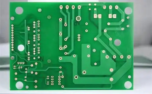
PCB board
2. Large interference signal in RF circuit simulation
The receiver must be sensitive to small signals, even if there are large interfering signals (blockers). This happens when a nearby powerful transmitter broadcasts on an adjacent channel and tries to receive weak or long-distance transmission. The interference signal may be 60-70 dB larger than the required signal, and may block the normal signal reception, resulting in a large amount of coverage of the input stage of the receiver, or excessive noise generated by the receiver at the input stage. If the receiver is driven to the nonlinear region by the interference source in the input phase, the above two problems will occur. To avoid these problems, the front end of the receiver must be very linear. Recall that "linearity" is also an important consideration when designing a receiver on a PCB. Since the receiver is a narrowband circuit, nonlinearity is measured as "intermodulation distortion". This includes driving the input signal with two sine or cosine waves with similar frequencies, and then measuring the intermodulation product. In general, SPICE is a time-consuming and expensive simulation software, because it must perform many loops to obtain the required frequency resolution to understand the distortion.
3. RF circuit analog expected signal is small
The receiver must be very sensitive to detect small input signals. Generally, the input power of the receiver can be as small as 1 ¼ V。 The sensitivity of the receiver is limited by the noise generated by the input circuit. Recall that noise is an important consideration when designing a receiver on a PCB. In addition, the ability to predict noise using simulation tools is critical. Figure 1 shows a typical superheterodyne receiver. The received signal is filtered and the input signal is amplified by a low noise amplifier (LNA). The signal is then mixed with a local oscillator (LO) to convert the signal to intermediate frequency (IF). The noise efficiency of front-end circuit mainly depends on LNA, mixer and LO. Although LNA noise can be found using traditional SPICE noise analysis, it is useless for mixers and LOs because the noise in these blocks will be seriously affected by larger LO signals. Small input signals require the receiver to have very large amplification, typically up to 120 dB. At such a high gain, any signal coupled from the output back to the input can cause problems. An important reason for using the superheterodyne receiver structure is that it distributes the gain over several frequencies to reduce the chance of coupling. This also makes the local oscillator frequency different from the frequency of the input signal, preventing the big interference signal from "polluting" the small input signal. For different reasons, in some wireless communication systems, direct conversion or homodyne structure can replace superheterodyne structure. In this architecture, the RF input signal is directly converted to the fundamental frequency in one step, and most of the gain is located at the fundamental frequency. The LO frequency is the same as the input signal frequency. In this case, it is necessary to understand the impact of a small amount of coupling, and a detailed model of "stray signal path" must be established, such as coupling (bonding wire) through substrate, package pin and bonding wire, and coupling through power line.
4. Adjacent channel interference in RF circuit simulation

Distortion also plays an important role in transmitters The nonlinearity generated by the transmitter at the output circuit may extend the bandwidth of the transmitted signal to adjacent frequency channels This phenomenon is called "spectral regeneration" Before the signal reaches the power amplifier (PA) of the transmitter, its bandwidth is limited; However, the "intermodulation distortion" in the PA leads to new bandwidth If too much bandwidth is added, the transmitter will be unable to meet the power requirements of its adjacent channels It is practically impossible to predict spectral regeneration using SPICE when transmitting digitally modulated signals Because the transmission operation of about 1000 digital symbols must be analogized to obtain representative spectrum, and high-frequency carriers need to be combined, which makes SPICE transient analysis on PCB


Just upload Gerber files, BOM files and design files, and the KINGFORD team will provide a complete quotation within 24h.