
Professional PCB manufacturing and assembly
Building 6, Zone 3, Yuekang Road,Bao'an District, Shenzhen, China
+86-13410863085Mon.-Sat.08:00-20:00

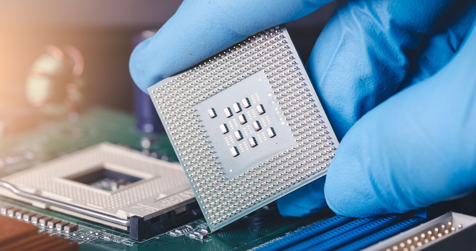
Shenzhen PCB manufacturers report the chip market and chip industry for you.
The chip industry is no stranger to streaming. The so-called wafer is to make chips through a series of process steps like a pipeline, which is in the middle stage of chip design and chip mass production and is the key link of chip manufacturing.
To put it simply, it is to submit the designed scheme to the chip manufacturer, who will produce several dozens of samples, check whether the designed chip can be used, and then optimize it. If the test is passed, mass production will start as follows.
Therefore, in order to test whether the integrated circuit design is successful, it must be taped. This is also an important reason why chip design enterprises generally need to invest a lot of costs in the early stage.
Streaming is a key link from design to mass production of a chip. When the chip is completely designed, it needs to be etched on the wafer according to the drawing. What kind of manufacturing process is used, what size of wafer, and the complexity of the chip will affect the success rate and cost of the chip. In addition, many chips can not be successfully streamed at one time, and it often requires multiple streamers to obtain ideal results.
However, streaming is a very expensive business. If you fail to do so many times, the company may collapse. In 2019, it was reported that Pembert S2 series chips of Pinecone Electronics, owned by Xiaomi, failed to be streamed for five consecutive times and the design team was reorganized.
There are chip manufacturers who have calculated this account. For 14nm process chips, it will cost about US $3 million to roll, for 7nm process chips, it will cost US $30 million to roll, and for 5nm process chips, it will cost US $47.25 million to roll. It can be seen that streaming is a huge expense for chip design enterprises, especially for small and medium-sized enterprises in the industry. The actual price of streaming is much higher than that of large factories, which makes the "life" not rich even worse.
Why are streamers so expensive?
Why is the price of the chip so expensive? This will mention the principle of chip manufacturing.
Chip manufacturing requires placing hundreds of millions of transistors in very small chips. The manufacturing process has reached the nanometer level and can only be completed by photolithography. Photolithography is to use light to carve the desired pattern. Photolithography requires the use of a mask (also known as a mask). The mask is to carve the designed circuit diagram on it, so that the pattern can be carved on the wafer after the light passes.
On the one hand, the chip is expensive because there are many processes that need to be verified at the beginning. From a circuit diagram to a chip, check whether each process step is feasible and whether the circuit has the required performance and functions. The chip streaming process lasts for at least three months (including raw material preparation, photolithography, doping, electroplating, and packaging test). Generally, it goes through more than 1000 processes, and the production cycle is long. Therefore, it is also the most important and costly link in chip manufacturing.
If it is successful, chips can be made on a large scale; On the contrary, it is necessary to find out the causes and carry out corresponding optimization design.
Among them, the chip chip is expensive, mainly in the mask and the wafer. These two items are expensive and are consumables. The mask is the most expensive. The price of the mask for a set of mid-range process is about 500000 dollars, and the price of a wafer is also thousands of dollars.
Are masks or wafers expensive?
The mask plate is made of quartz, which is a graphic transfer tool or master plate in the microelectronic manufacturing process. Its function is similar to the "negative" of traditional cameras. According to the graphics required by customers, micro and nano scale fine graphics are engraved on the mask plate through the photolithography process, which is the carrier of graphic design, process technology and other contents.
Then imagine the process of converting the mask graphics to the wafer as the workflow of the banknote printing machine. Think of the lithography machine as a banknote printing machine. The wafer is equivalent to banknote printing paper, and the mask is a printing plate. The process of printing the graphics of the banknote master onto the paper is just like the lithography machine printing the chip graphics on the mask onto the wafer.
Photolithography requires mask plate, which is used to carve the designed circuit diagram on it, so that after the light passes, the pattern can be carved on the wafer.
The quality of mask will directly affect the quality of lithography, and manufacturing defects and errors on mask will also be introduced into chip manufacturing along with the lithography process. Therefore, mask is one of the decisive factors for the accuracy and quality of downstream products.
The price of mask mainly depends on the "process node" selected by the chip. The higher the process node is, the more expensive the film will be. This is because the more advanced the process node, the more mask layers need to be used. It is understood that about 60 masks are required for the 14nm process, and 80 or even hundreds of masks may be required for the 7nm process.
The number of mask layers is more, not only because the mask plate is expensive, but also because every additional layer of "mask plate" will require one more "lithography", one more "photoresist", one more "exposure", and then one more "development". The cost of the whole process will be greatly increased.
According to IBS data, the cost of the mask used in the 16/14nm process is about US $5 million. By the 7nm process, the cost of the mask quickly rose to US $15 million.
The total cost of the mask, including the cost of raw materials such as quartz and photoresist, the use cost of the mask writer and inspection machines, and the generation of mask related data, including the cost of OPC, MDP and other software licensing, server use and manual development. For a chip, the mask with dozens of layers often requires so many steps, and equipment, software and personnel are indispensable, so the cost is naturally expensive.
The cost of mask takes a large part in the film production, because in the early stage of film production, 5-25 pieces are produced for product verification, and the main cost is mask cost. Correspondingly, during formal production, the cost of Mask is only counted once. There are a large number of wafers that can share the cost, which is naturally cheap.
To be exact, the average cost of each chip is cheaper, not the total cost of streaming.
According to insiders, the cost of 40nm wafers in a Foundry is about US $600000 to US $900000. Mask accounts for the majority, about 600000 to 900000 dollars; The cost of each wafer is about 3000-4000 dollars.
Therefore, if 10 wafers are produced, the cost of each wafer is (900000+4000 * 10)/10=94000 dollars; However, if 10000 wafers are produced, the cost of each wafer is (900000+4000 * 10000)/10000=4090 dollars.
It can be seen that after mass production, tens of thousands of wafers will be produced, and each wafer may be about 3000-4000 dollars. After the cost of Mask is shared equally with each wafer, it will be very small. At this time, the cost of the wafer is the main source of cost. Therefore, if only a small amount of film is produced, the mask cost is the main factor. On the contrary, if there is a lot of mass production, it is the dominant cost of wafers.
In addition, the machines in semiconductor manufacturers are cheap for millions of dollars and expensive for hundreds of millions of dollars. It is understood that the 28 nm Mask machine is more than 50 million US dollars each, and it will take seven years to complete the depreciation of these instruments. That is to say, about 14% of the machine value will be lost after one year of use.
The depreciation life of equipment in wafer foundry industry is usually 5-7 years. It is reported that SMIC's depreciation expense in 2019 exceeded 1.4 billion, mainly because the investment in advanced manufacturing processes requires the purchase of some machinery and equipment with higher unit prices, which makes the depreciation expense increase year by year. In 2021, TSMC's depreciation expense will reach nearly NT $100 billion, the highest in history.
In terms of the process R&D cycle, the cost and depreciation expense of the machine are already very high, but it is also a challenging task to adjust the yield and reliability of the process to the requirements of mass production. (It is reported that a factory has set up 28nm, and all the machines will be in place in 2011/2012, but the yield has not been adjusted to the strict mass production standard five or six years later, which shows how difficult it is. At the same time, it has also lost many years of equipment depreciation costs in vain.)
Secondly, there are labor costs, maintenance costs and consumables, which are the reasons for the high cost of Mask.
According to the report of etnews, as the current supply and demand situation worsens, the price of the mask is still rising, and the delivery time has been repeatedly postponed. Even if you pay extra fees, it is difficult to buy the mask in time. The delivery time, which usually takes 4-7 days, has recently increased to 14 days, and the delivery time of some enterprises has been extended to 7 times of the original.
In addition, in order to keep up with Moore's Law, Foundry's investment in equipment and technology R&D for upgrading and upgrading is increasing. Because Foundry's huge investment in advanced production lines, its costs will inevitably be passed on to customers' project costs. This has also led to the rising cost of chip manufacturing.
How to reduce the cost of film?
Influenced by the above factors, the cost of chip streaming has become a difficult problem for design enterprises. So, in the face of the high price of streaming, is there any way to reduce the cost?
Wang Long, senior director of Moore Elite, said to the author that MPW (Multi Project Wafer) is a streaming method that can help design enterprises reduce costs. MPW means that multiple projects share a certain wafer, the same manufacturing process can undertake the manufacturing tasks of multiple IC designs, and multiple IC designs using the same process can be streamed on the same wafer. After manufacturing, each design can obtain dozens of chip samples, which is sufficient for experiments and tests in the prototype design stage.
Generally speaking, several companies or institutions purchase a set of masks together, and then several chips will exist on the same wafer produced. After the wafer is cut, they will "take home" their chips. The manufacturing cost is shared by all MPW projects according to chip area, which greatly reduces the risk of product development.
According to insiders, MPW has a certain process, which is usually organized by wafer foundries or third-party service organizations. The MPW time points of various processes in a certain year are preset. Generally, the more advanced the process, the higher the frequency of MPW. The wafer foundry will divide the wafer into several regions and make a quotation in advance, and each company will book one or more regions according to its own situation.
For participants, there is a certain pressure on the progress of design and development. However, in contrast, the benefits of MPW are obvious. The use of multi project wafers can reduce the production cost of chips, provide practical opportunities for designers, and promote the transformation of chip design results. It has a considerable role in promoting the training of IC design talents, the development of small and medium-sized design companies, and the development of new products.
By contrast, the advantage of sharing masks is to save money, but it may take more time to wait for the time node of the OEM. For those enterprises who are not poor in money or are in a hurry, they can certainly use a set of masks (Full Mask). All masks in the manufacturing process serve their own design, and are usually used in the mass production stage after design finalization. When the machine goes off, gold is ten thousand liang.
However, in the current situation of severe capacity shortage, the OEM has completely different attitudes towards different customers' product needs, competitive advantages, market prospects and plans. The OEM will make judgments based on the overall consideration of the customer's order quantity, the stability of subsequent orders and the market prospects of the products.
In fact, for most SMEs, in addition to price, they also face many challenges, including production capacity and delivery time, in the streaming or mass production link:
1. Do not know Foundry system, lack experience in process selection and dealing with Foundry;
2. The entry threshold of mainstream Foundry is high, and it is difficult for emerging players to apply for the expected process or support, resulting in high communication costs;
3. Lack of systematic supply chain management capability, especially in the ramp up stage of mass production capacity, being overly optimistic about capacity, delivery date and quality;
4. In the case of capacity shortage, there is a lack of stock mechanism, and panicked orders or orders are placed again when there is an order, resulting in capacity not keeping up with market demand. In addition, changes in delivery dates and capacity fluctuations will greatly increase the communication costs between startups and foundries, reducing efficiency.
In this regard, small and medium-sized chip design enterprises can seek the cooperation of third-party operation service agencies with resources, strength and experience to solve the supply chain problems encountered.
Write at the end
A chip development project needs to go through a long process from product definition, design, verification and simulation to final streaming. As the "final exam", streaming may fail due to any minor negligence in the long process before, but once the streaming fails, it means that the enterprise will face losses from tens of millions of dollars and market opportunities for at least half a year.
This is an unbearable pain for many enterprises.
In this regard, chip design enterprises, manufacturers and relevant industry service platforms and institutions should work closely to complement each other's advantages and work together to solve the "streaming problem" that plagues developers.
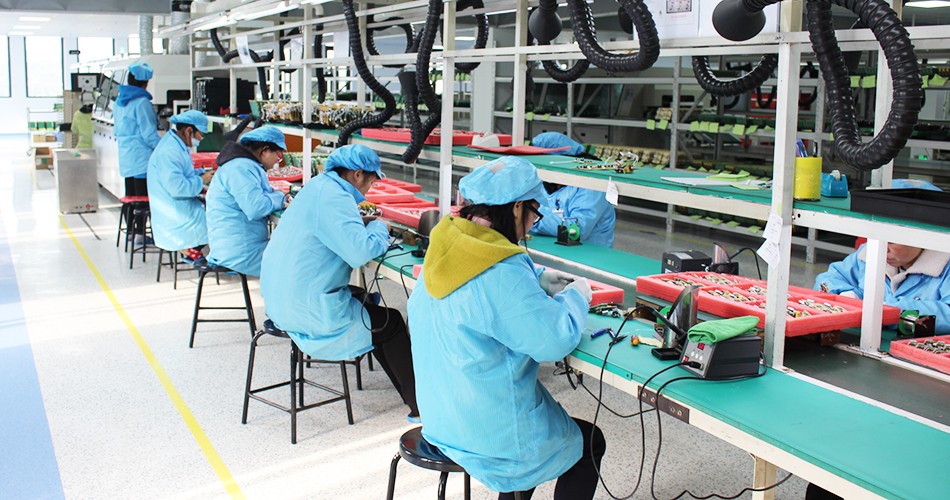


Just upload Gerber files, BOM files and design files, and the KINGFORD team will provide a complete quotation within 24h.