
Professional PCB manufacturing and assembly
Building 6, Zone 3, Yuekang Road,Bao'an District, Shenzhen, China
+86-13410863085Mon.-Sat.08:00-20:00

The main differences between wave soldering and reflow welding (reflow soldering) are:
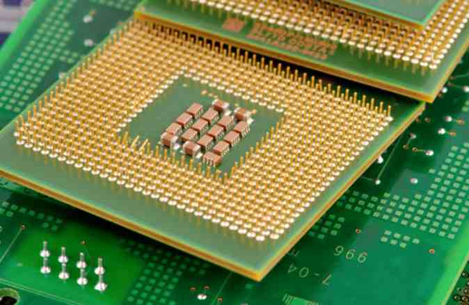
1, wave soldering is to dissolve the tin strip into a liquid state through the tin tank, use the motor to form a wave peak, so that the PCB and the parts are welded together, generally used in the hand plug-in (DIP) welding and smt glue board. Reflow welding is mainly used in the SMT industry, which melts and welds the solder paste printed on the PCB through hot air or other thermal radiation conduction.
2, their process is different: wave soldering to first spray flux, and then through preheating, welding, cooling zone.
Reflow welding (reflow welding) through the preheating zone, reflow zone, cooling zone.
In addition, wave soldering is suitable for hand insert plate and dispensing plate, and requires all components to be heat-resistant, over the crest surface can not have SMT solder paste components, SMT solder paste board can only be over flow welding (reflow soldering), can not use the crest Welding.
The following is a comparison of the process of wave soldering and reflow welding (reflow welding) :
1. Wave soldering process - first print or drip a trace of patch adhesive (insulation adhesive) to the bottom or edge of the printed board components (patch adhesive can not pollute the printed board pad and the end of the components), and then attach the chip components to the position specified on the surface of the printed board, and then put the printed board with mounted components on the conveyor belt of the reflow welding equipment. Glue curing. The cured component is firmly bonded to the printed board. Then the discrete components are inserted, and finally the wave crest welding is carried out simultaneously with the inserted components.

2. Reflow welding process -- first print or drip a trace of lead-tin solder paste onto the pad of the printed board, then paste the chip components on the specified position on the surface of the printed board, and finally place the printed board with affixed components on the conveyor belt of the reflow welding equipment. From the furnace inlet to the outlet, it takes about 5-6 minutes to complete the drying, preheating, melting, cooling and all welding processes.
Reflow welding (reflow soldering) principle
1. When the PCB enters the heating zone (dry zone), the solvent and gas in the solder paste evaporate. At the same time, the flux in the solder paste moistens the solder pad, component ends and pins, the solder paste softers, collapses and covers the solder pad, and the solder pad and component pins are isolated from oxygen.
2. When the PCB enters the insulation area, the PCB and components are fully preheated to prevent the PCB from suddenly entering the welding high temperature area and damaging the PCB and components.
3. When the PCB enters the welding zone, the temperature rises rapidly so that the solder paste reaches a molten state, and the liquid solder wets, diffuses, flows or mixes with the solder joints to form solder joints on the PCB pad, component ends and pins.
4. The PCB enters the cooling zone to solidify the solder joint. At this point, the reflow welding is completed.
When the temperature of a high Tg printed circuit board rises to a certain threshold, the substrate will change from a "glass state" to a "rubber state", and the temperature at this time is called the glass transition temperature (Tg) of the board. In other words, Tg is the highest temperature (° C) at which the substrate remains rigid. That is to say, ordinary PCB substrate materials at high temperatures, continue to produce softening, deformation, melting and other phenomena, but also in the mechanical, electrical characteristics of the sharp decline, which affects the service life of the product, the general Tg plate is more than 130 ° C, high Tg is generally greater than 170 ° C, medium Tg is about more than 150 ° C; Usually Tg≥170℃ PCB printed board, called high Tg printed board; The Tg of the substrate is increased, and the heat resistance, moisture resistance, chemical resistance, and stability of the printed board will be improved and improved.
The higher the TG value, the better the temperature resistance of the plate, especially in the lead-free process, high Tg is more applied; High Tg means high heat resistance. With the rapid development of the electronics industry, especially the electronic products represented by computers, towards the development of high function and high multilayer, the higher heat resistance of PCB substrate materials is required as the premise. The emergence and development of high-density installation technology represented by SMT and CMT has made PCB more and more inseparable from the support of high heat resistance of the substrate in terms of small aperture, fine wiring and thin shape.


Just upload Gerber files, BOM files and design files, and the KINGFORD team will provide a complete quotation within 24h.