
Professional PCB manufacturing and assembly
Building 6, Zone 3, Yuekang Road,Bao'an District, Shenzhen, China
+86-13410863085Mon.-Sat.08:00-20:00

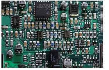
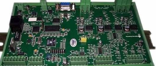
In PCB design, wiring is a crucial step. Reasonable and effective wiring can ensure the stability and reliability of the circuit and avoid the adverse effects of circuit wiring errors. In the PCB layout design, you need to follow certain rules and principles, kinhford Electronics is a professional PCB design company, the following we will introduce the six routing rules in PCB design.
")
First: According to the transmission signal speed classification
In the wiring need to be classified according to the different signal transmission speed. In general, the faster the transmission speed of the signal requires a shorter line distance to avoid distortion and interference during signal propagation. Therefore, when wiring, it is necessary to determine which signals are faster, and then arrange them closer to the chip.
Second: sub-regional layout
For different functional modules, it is necessary to arrange them in different areas to gather devices with the same function together for easy management and maintenance. In the wiring, it is necessary to avoid the crossing of different functions in the same layer, causing interference and signal distortion.
Third: Keep your distance
A certain distance should be maintained between different signals to avoid crosstalk and mutual interference between signals. For different signal types, the distance to be maintained needs to be determined according to its characteristics. For example, the distance between the signals encountered by the same layer should be more than 2mm, and the distance between the ground and the power cord can be slightly shorter.
Fourth: Prevent too long and bending
Long track and zigzag track will affect the signal quality, resulting in signal distortion and interference. In order to avoid this situation, it is necessary to avoid the occurrence of too long and too curved. For some lines that need to be bent, excessive curves are added at the bend to alleviate electromagnetic fatigue.
Fifth: layered wiring
For high-density PCB wiring, layering is required. In this way, the wiring of different functional modules can be unloaded into different layers to avoid cross interference. At the same time, layering can also save a certain amount of space, making the PCB board more compact.
Sixth: ground wiring
In PCB design, ground wiring is a more important part. For high-speed digital signals and analog signals, it is generally necessary to conduct ground wiring independently. Especially in the case of serious signal interference, grounding wiring can effectively reduce interference and noise.
In short, the wiring in PCB design is very important, and it needs to follow some rules and principles. Among them, classification and sub-regional layout are the most critical two points, and attention needs to be paid to maintaining distance, preventing excessive length and bending, layered wiring and ground wiring. Only when PCB routing is designed in strict accordance with these rules can the stability and reliability of the circuit be ensured.
What does SMT do?
Jun 16,2023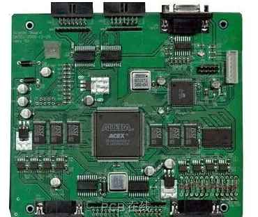


Just upload Gerber files, BOM files and design files, and the KINGFORD team will provide a complete quotation within 24h.