
Professional PCB manufacturing and assembly
Building 6, Zone 3, Yuekang Road,Bao'an District, Shenzhen, China
+86-13410863085Mon.-Sat.08:00-20:00

1. Power supply, ground processing
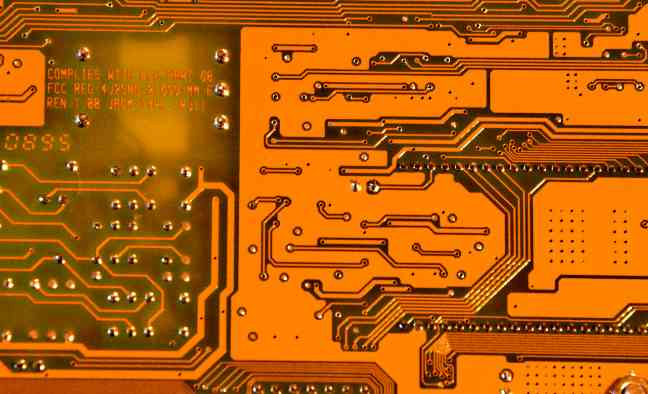
Even if the wiring in the entire PCB board is completed well, the interference caused by the inconsiderate power supply and ground wire will reduce the performance of the product, and sometimes even affect the success rate of the product. Therefore, the wiring of electricity and ground wires should be taken seriously, and the noise interference caused by electricity and ground wires should be reduced to a minimum to ensure the quality of products. For every engineer who is engaged in the design of electronic products, it is understood that the cause of the noise between the ground line and the power line is generated, and only the reduced noise suppression is described: it is well known that the decoupling capacitor is added between the power supply and the ground line. Try to widen the width of the power supply and ground wire, it is best that the ground wire is wider than the power cord, and their relationship is:
Ground > Power line > Signal line, usually signal line width is: 0.2 ~ 0.3mm, the maximum width can reach 0.05 ~ 0.07mm, the power line is 1.2 ~ 2.5mm, the PCB of the digital circuit can be composed of a wide ground wire loop, That is to form a ground network to use (analog circuit can not be used in this way) with a large area of copper layer for ground, in the printed board is not used to connect with the ground as ground. Or make a multi-layer board, the power supply, the ground line occupy a layer.

2. Common ground processing of digital circuit and analog circuit
There are now many PCBS that are no longer single-function circuits (digital or analog circuits), but are composed of a mixture of digital and analog circuits. Therefore, when wiring, it is necessary to consider the interference between them, especially the noise interference on the ground wire. The frequency of the digital circuit is high, the sensitivity of the analog circuit is strong, for the signal line, the high-frequency signal line is as far away from the sensitive analog circuit device as possible, for the ground line, the PCB has only one node to the outside world, so it must be processed inside the PCB, the problem of the number and mode common ground, and the digital and analog inside the board are actually separated from each other. Only at the interface between the PCB and the outside world (such as plugs, etc.). There is a bit of a short connection between digital and analog, but note that there is only one connection point. There are also common on the PCB, which is determined by the system design.
3, the signal line is distributed on the electrical (ground) layer in the multi-layer printed board wiring, because the signal line layer is not finished the line is not much, and then more layers will cause waste will also increase the production of a certain amount of work, the cost has increased accordingly, in order to solve this contradiction, you can consider wiring on the electrical (ground) layer. The power layer should be considered first, followed by the formation. Because it is better to preserve the integrity of the formation.
4, the large-area conductor in the connection leg treatment, in the large-area grounding (electrical), the commonly used components of the leg connection with its connection, the treatment of the connection leg needs comprehensive consideration, in terms of electrical performance, the leg of the welding pad and copper surface full connection is good, but the welding assembly of the components there are some bad hidden dangers such as: ① welding requires high-power heater. ② Easy to cause virtual solder joints. Therefore, taking into account the electrical performance and process needs, make a cross welding pad, called heat shield, commonly known as Thermal pad, in this way, the possibility of virtual solder joints caused by excessive heat dissipation in the welding section is greatly reduced. The treatment of the electrical (ground) leg of the multilayer board is the same.
5, the role of the network system in wiring In many CAD systems, wiring is determined according to the network system. The grid is too dense, although the path has increased, the step is too small, and the amount of data in the graph field is too large, which inevitably has higher requirements for the storage space of the device, and also has a great impact on the computing speed of the object computer electronic products. Some paths are not valid, such as those occupied by the pads of the component legs or by mounting holes or fixing holes. Too sparse grid and too few channels have great influence on the distribution flux. Therefore, it is necessary to have a reasonable grid system to support the wiring. The distance between the legs of the standard components is 0.1 inches (2.54mm), so the basis of the grid system is generally set at 0.1 inches (2.54mm) or an integral multiple of less than 0.1 inches, such as: 0.05 inches, 0.025 inches, 0.02 inches, etc.
6, design rules check (DRC) After the wiring design is completed, it is necessary to carefully check whether the wiring design meets the rules formulated by the designer, and it is also necessary to confirm whether the rules formulated meet the needs of the printed board production process, the general inspection has the following aspects: Whether the distance between wire and wire, wire and component pad, wire and through hole, component pad and through hole, through hole and through hole is reasonable, whether it meets the production requirements. Is the width of the power line and ground line appropriate, and is there a tight coupling between the power supply and ground line (low wave impedance)? Is there any place in the PCB that can make the ground wire wider? Whether the best measures are taken for the key signal lines, such as the shortest length, the protection line, the input line and the output line are clearly separated. Whether the analog circuit and the digital circuit have their own ground lines.
Modify some undesirable lines. Is there a process line on the PCB? Whether the solder resistance meets the requirements of the production process, whether the solder resistance size is appropriate, whether the character mark is pressed on the device pad, so as not to affect the quality of Denso. Whether the edge of the outer frame of the power supply layer in the multi-layer board is reduced, such as the copper foil of the power supply layer is exposed outside the board, which is easy to cause short circuit. Overview The purpose of this document is to explain the process and some considerations for a working group for designing printed boards using the PADS printed board design software PowerPCB.


Just upload Gerber files, BOM files and design files, and the KINGFORD team will provide a complete quotation within 24h.